参数资料
| 型号: | 24LC128-E/P |
| 厂商: | Microchip Technology |
| 文件页数: | 5/38页 |
| 文件大小: | 0K |
| 描述: | IC EEPROM 128KBIT 400KHZ 8DIP |
| 产品培训模块: | I2C Serial EEPROM |
| 标准包装: | 60 |
| 格式 - 存储器: | EEPROMs - 串行 |
| 存储器类型: | EEPROM |
| 存储容量: | 128K (16K x 8) |
| 速度: | 400kHz |
| 接口: | I²C,2 线串口 |
| 电源电压: | 2.5 V ~ 5.5 V |
| 工作温度: | -40°C ~ 125°C |
| 封装/外壳: | 8-DIP(0.300",7.62mm) |
| 供应商设备封装: | 8-PDIP |
| 包装: | 管件 |
第1页第2页第3页第4页当前第5页第6页第7页第8页第9页第10页第11页第12页第13页第14页第15页第16页第17页第18页第19页第20页第21页第22页第23页第24页第25页第26页第27页第28页第29页第30页第31页第32页第33页第34页第35页第36页第37页第38页
�� �
�
�24AA128/24LC128/24FC128�
�2.0�
�PIN� DESCRIPTIONS�
�The� descriptions� of� the� pins� are� listed� in� Table� 2-1.�
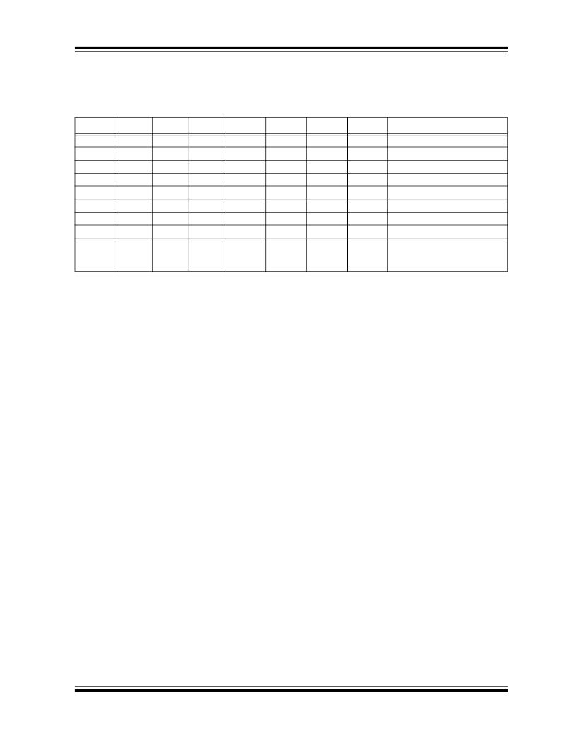
�TABLE� 2-1:�
�PIN� FUNCTION� TABLE�
�Name�
�A0�
�A1�
�(NC)�
�A2�
�V� SS�
�SDA�
�SCL�
�WP�
�V� CC�
�PDIP�
�1�
�2�
�—�
�3�
�4�
�5�
�6�
�7�
�8�
�SOIC�
�1�
�2�
�—�
�3�
�4�
�5�
�6�
�7�
�8�
�TSSOP�
�1�
�2�
�—�
�3�
�4�
�5�
�6�
�7�
�8�
�MSOP�
�—�
�—�
�1,� 2�
�3�
�4�
�5�
�6�
�7�
�8�
�DFN� (1)�
�1�
�2�
�—�
�3�
�4�
�5�
�6�
�7�
�8�
�TDFN� (1)�
�1�
�2�
�—�
�3�
�4�
�5�
�6�
�7�
�8�
�CS�
�3�
�2�
�—�
�5�
�8�
�6�
�7�
�4�
�1�
�Function�
�User� Configurable� Chip� Select�
�User� Configurable� Chip� Select�
�Not� Connected�
�User� Configurable� Chip� Select�
�Ground�
�Serial� Data�
�Serial� Clock�
�Write-Protect� Input�
�+1.7V� to� 5.5V� (24AA128)�
�+2.5V� to� 5.5V� (24LC128)�
�+1.7V� to� 5.5V� (24FC128)�
�Note� 1:�
�The� exposed� pad� on� the� DFN/TDFN� package� can� be� connected� to� V� SS� or� left� floating.�
�2.1�
�A0,� A1,� A2� Chip� Address� Inputs�
�2.3�
�Serial� Clock� (SCL)�
�The� A0,� A1� and� A2� inputs� are� used� by� the� 24XX128� for�
�multiple� device� operations.� The� levels� on� these� inputs�
�This� input� is� used� to� synchronize� the� data� transfer� to�
�and� from� the� device.�
�are� compared� with� the� corresponding� bits� in� the� slave�
�address.� The� chip� is� selected� if� the� compare� is� true.�
�2.4�
�Write-Protect� (WP)�
�For� the� MSOP� package� only,� pins� A0� and� A1� are� not�
�connected.�
�Up� to� eight� devices� (two� for� the� MSOP� package)� may�
�be� connected� to� the� same� bus� by� using� different� Chip�
�Select� bit� combinations.� These� inputs� must� be�
�This� pin� must� be� connected� to� either� V� SS� or� V� CC� .� If� tied�
�to� V� SS� ,� write� operations� are� enabled.� If� tied� to� V� CC� ,�
�write� operations� are� inhibited� but� read� operations� are�
�not� affected.�
�connected� to� either� V� CC� or� V� SS� .�
�3.0�
�FUNCTIONAL� DESCRIPTION�
�In� most� applications,� the� chip� address� inputs� A0,� A1�
�and� A2� are� hard-wired� to� logic� ‘� 0� ’� or� logic� ‘� 1� ’.� For�
�applications� in� which� these� pins� are� controlled� by� a�
�microcontroller� or� other� programmable� device,� the� chip�
�address� pins� must� be� driven� to� logic� ‘� 0� ’� or� logic� ‘� 1� ’�
�before� normal� device� operation� can� proceed.�
�The� 24XX128� supports� a� bidirectional� 2-wire� bus� and�
�data� transmission� protocol.� A� device� that� sends� data�
�onto� the� bus� is� defined� as� a� transmitter� and� a� device�
�receiving� data� as� a� receiver.� The� bus� must� be�
�controlled� by� a� master� device� which� generates� the�
�Serial� Clock� (SCL),� controls� the� bus� access� and�
�2.2�
�Serial� Data� (SDA)�
�generates� the� Start� and� Stop� conditions� while� the�
�24XX128� works� as� a� slave.� Both� master� and� slave� can�
�This� is� a� bidirectional� pin� used� to� transfer� addresses�
�and� data� into� and� out� of� the� device.� It� is� an� open� drain�
�terminal.� Therefore,� the� SDA� bus� requires� a� pull-up�
�resistor� to� V� CC� (typical� 10� k� ?� for� 100� kHz,� 2� k� ??� for�
�400� kHz� and� 1� MHz).�
�For� normal� data� transfer,� SDA� is� allowed� to� change�
�only� during� SCL� low.� Changes� during� SCL� high� are�
�reserved� for� indicating� the� Start� and� Stop� conditions.�
�?� 2010� Microchip� Technology� Inc.�
�operate� as� a� transmitter� or� receiver,� but� the� master�
�device� determines� which� mode� is� activated.�
�DS21191S-page� 5�
�相关PDF资料 |
PDF描述 |
|---|---|
| XC2V250-4FG256I | IC FPGA VIRTEX-II 256FGBGA |
| 25LC320/P | IC EEPROM 32KBIT 2MHZ 8DIP |
| XC2V250-5FGG256C | IC FPGA VIRTEX-II 250K 256-FBGA |
| RCB92DHBR-S329 | EDGECARD PCI 184PS .050 R/A 3.3V |
| XC2V250-4FGG256I | IC FPGA VIRTEX-II 250K 256-FBGA |
相关代理商/技术参数 |
参数描述 |
|---|---|
| 24LC128ESM | 制造商:MICROCHIP 制造商全称:Microchip Technology 功能描述:128K I 2 C ⑩ CMOS Serial EEPROM |
| 24LC128-ESM | 制造商:MICROCHIP 制造商全称:Microchip Technology 功能描述:I2C⑩ Serial EEPROM Family Data Sheet |
| 24LC128ESN | 制造商:MICROCHIP 制造商全称:Microchip Technology 功能描述:128K I 2 C ⑩ CMOS Serial EEPROM |
| 24LC128-ESN | 制造商:MICROCHIP 制造商全称:Microchip Technology 功能描述:I2C⑩ Serial EEPROM Family Data Sheet |
| 24LC128EST | 制造商:MICROCHIP 制造商全称:Microchip Technology 功能描述:128K I 2 C ⑩ CMOS Serial EEPROM |
发布紧急采购,3分钟左右您将得到回复。