- 您现在的位置:买卖IC网 > PDF目录155701 > 24LC320-IP (Microchip Technology Inc.) 32K 2.5V SPI Bus Serial EEPROM PDF资料下载
参数资料
| 型号: | 24LC320-IP |
| 厂商: | Microchip Technology Inc. |
| 英文描述: | 32K 2.5V SPI Bus Serial EEPROM |
| 中文描述: | 32K的2.5V的SPI总线串行EEPROM |
| 文件页数: | 8/12页 |
| 文件大小: | 87K |
| 代理商: | 24LC320-IP |
1996 Microchip Technology Inc.
Preliminary
DS21158B-page 5
25LC320
2.0
PRINCIPLES OF OPERATION
The 25LC320 is a 4096 byte EEPROM designed to
interface directly with the serial peripheral interface
(SPI
) port of many of today’s popular microcontroller
families, including Microchip’s midrange PIC16CXX
microcontrollers. It may also interface with microcontrol-
lers that do not have a built-in SPI
port by using dis-
crete I/O lines programmed properly with software.
The 25LC320 contains an 8-bit instruction register. The
part is accessed via the SI pin, with data being clocked
in on the rising edge of SCK. If the WPEN bit in the Sta-
tus Register is set, the WP pin must be held high to
allow writing to the non-volatile bits in the status regis-
ter.
Table 2-1 contains a list of the possible instruction bytes
and format for device operation. All instructions,
addresses and data are transferred MSB rst, LSB last.
Data is sampled on the rst rising edge of SCK after CS
goes low. If the clock line is shared with other peripheral
devices on the SPI
bus, the user can assert the
HOLD input and place the 25LC320 in ‘HOLD’ mode.
After releasing the HOLD pin, operation will resume
from the point when the HOLD was asserted.
2.1
Write Enable (WREN) and Write
Disable (WRDI)
The 25LC320 contains a write enable latch. This latch
must be set before any write operation will be
completed internally. The WREN instruction will set the
latch, and the WRDI will reset the latch. The following is
a list of conditions under which the write enable latch
will be reset:
Power-up
WRDI instruction successfully executed
WRSR instruction successfully executed
WRITE instruction successfully executed
2.2
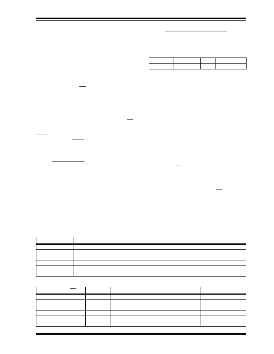
Read Status Register (RDSR)
The RDSR instruction provides access to the status
register. The status register may be read at any time,
even during a write cycle. The status register is format-
ted as follows:
The Write-In-Process (WIP) bit indicates whether the
25LC320 is busy with a write operation. When set to a
‘1’ a write is in progress, when set to a ‘0’ no write is in
progress. This bit is read only.
The Write Enable Latch (WEL) bit indicates the status
of the write enable latch. When set to a ‘1’ the latch
allows writes to the array and status register, when set
to a ‘0’ the latch prohibits writes to the array and status
register. The state of this bit can always be updated via
the WREN or WRDI commands regardless of the state
of write protection on the status register. This bit is read
only.
The Block Protection (BP0 and BP1) bits indicate
which blocks are currently write protected. These bits
are set by the user issuing the WRSR instruction.
These bits are non-volatile.
The Write Protect Enable (WPEN) bit is a non-volatile
bit that is available as an enable bit for the WP pin. The
Write Protect (WP) pin and the Write Protect Enable
(WPEN)
bit
in
the
status
register
control
the
programmable
hardware
write
protect
feature.
Hardware write protection is enabled when WP pin is
low and the WPEN bit is high. Hardware write
protection is disabled when either the WP pin is high or
the WPEN bit is low. When the chip is hardware write
protected, only writes to non-volatile bits in the status
register are disabled. See Table 2-2 for matrix of
functionality on the WPEN bit and Figure 2-1 for a
owchart of Table 2-2. See Figure 3-5 for RDSR timing
sequence.
7
654
3
2
1
0
WPEN
X
BP1
BP0
WEL
WIP
TABLE 2-1:
INSTRUCTION SET
TABLE 2-2:
WRITE PROTECT FUNCTIONALITY MATRIX
Instruction Name
Instruction Format
Description
WREN
0000 0110
Set the write enable latch (enable write operations)
WRDI
0000 0100
Reset the write enable latch (disable write operations)
RDSR
0000 0101
Read status register
WRSR
0000 0001
Write status register (write protect enable and block write protection bits)
READ
0000 0011
Read data from memory array beginning at selected address
WRITE
0000 0010
Write data to memory array beginning at selected address
WPEN
WP
WEL
Protected Blocks
Unprotected Blocks
Status Register
0
X
0
Protected
0
X
1
Protected
Writable
1
Low
0
Protected
1
Low
1
Protected
Writable
Protected
X
High
0
Protected
X
High
1
Protected
Writable
相关PDF资料 |
PDF描述 |
|---|---|
| 24LC320-ISN | 32K 2.5V SPI Bus Serial EEPROM |
| 24LC320-IST | 32K 2.5V SPI Bus Serial EEPROM |
| 24LC320-P | CABLE BNC MALE RG-58C/U 300,1 |
| 24LC320-SN | 32K 2.5V SPI Bus Serial EEPROM |
| 24LC320-ST | 32K 2.5V SPI Bus Serial EEPROM |
相关代理商/技术参数 |
参数描述 |
|---|---|
| 24LC32A/P | 功能描述:电可擦除可编程只读存储器 4kx8 - 5V - 2.5V RoHS:否 制造商:Atmel 存储容量:2 Kbit 组织:256 B x 8 数据保留:100 yr 最大时钟频率:1000 KHz 最大工作电流:6 uA 工作电源电压:1.7 V to 5.5 V 最大工作温度:+ 85 C 安装风格:SMD/SMT 封装 / 箱体:SOIC-8 |
| 24LC32A/P | 制造商:Microchip Technology Inc 功能描述:IC EEPROM SERIAL 32K 24LC32 DIP8 |
| 24LC32A/S15K | 制造商:Microchip Technology Inc 功能描述:32K, 4K X 8, 2.5V SERIAL DIE IN WAFFLE PK - Gel-pak, waffle pack, wafer, diced wafer on film |
| 24LC32A/SM | 功能描述:电可擦除可编程只读存储器 4kx8 - 5V - 2.5V RoHS:否 制造商:Atmel 存储容量:2 Kbit 组织:256 B x 8 数据保留:100 yr 最大时钟频率:1000 KHz 最大工作电流:6 uA 工作电源电压:1.7 V to 5.5 V 最大工作温度:+ 85 C 安装风格:SMD/SMT 封装 / 箱体:SOIC-8 |
| 24LC32A/SM | 制造商:Microchip Technology Inc 功能描述:EEPROM SERIAL 32K 24LC32 SOIC8 |
发布紧急采购,3分钟左右您将得到回复。