- 您现在的位置:买卖IC网 > PDF目录49884 > 2N7236U (MICROSEMI CORP-LAWRENCE) 18 A, 100 V, 0.22 ohm, P-CHANNEL, Si, POWER, MOSFET, TO-267AB PDF资料下载
参数资料
| 型号: | 2N7236U |
| 厂商: | MICROSEMI CORP-LAWRENCE |
| 元件分类: | JFETs |
| 英文描述: | 18 A, 100 V, 0.22 ohm, P-CHANNEL, Si, POWER, MOSFET, TO-267AB |
| 封装: | SMD-1, U-PKG-3 |
| 文件页数: | 1/4页 |
| 文件大小: | 118K |
| 代理商: | 2N7236U |
TECHNICAL DATA SHEET
6 Lake Street, Lawrence, MA 01841
Gort Road Business Park, Ennis, Co. Clare, Ireland
1-800-446-1158 / (978) 620-2600 / Fax: (978) 689-0803
Tel: +353 (0) 65 6840044 Fax: +353 (0) 65 6822298
Website: http://www.microsemi.com
P-CHANNEL MOSFET
Qualified per MIL-PRF-19500/595
T4-LDS-0061 Rev. 2 (101873)
Page 1 of 4
DEVICES
LEVELS
2N7236
2N7236U
JAN
JANTX
JANTXV
ABSOLUTE MAXIMUM RATINGS (TC = +25°C unless otherwise noted)
Parameters / Test Conditions
Symbol
Value
Unit
Drain – Source Voltage
VDS
-100
Vdc
Gate – Source Voltage
VGS
± 20
Vdc
Continuous Drain Current
TC = +25°C
ID1
-18
Adc
Continuous Drain Current
TC = +100°C
ID2
-11
Adc
Max. Power Dissipation
TC = +25°C
Ptl
125 (1)
W
Drain to Source On State Resistance
Rds(on)
0.20 (2)
Ω
Operating & Storage Temperature
Top, Tstg
-55 to +150
°C
Note: (1) Derated Linearly by 1.0 W/°C for TC > +25°C
(2) VGS = 10Vdc, ID = -11A
ELECTRICAL CHARACTERISTICS (TA = +25°C, unless otherwise noted)
Parameters / Test Conditions
Symbol
Min.
Max.
Unit
OFF CHARACTERTICS
Drain-Source Breakdown Voltage
VGS = 0V, ID = 1mAdc
V(BR)DSS
-100
Vdc
Gate-Source Voltage (Threshold)
VDS ≥ VGS, ID = -0.25mA
VDS ≥ VGS, ID = -0.25mA, Tj = +125°C
VDS ≥ VGS, ID = -0.25mA, Tj = -55°C
VGS(th)1
VGS(th)2
VGS(th)3
-2.0
-1.0
-4.0
-5.0
Vdc
Gate Current
VGS = ±20V, VDS = 0V
VGS = ±20V, VDS = 0V, Tj = +125°C
IGSS1
IGSS2
±100
±200
nAdc
Drain Current
VGS = 0V, VDS = -80V
VGS = 0V, VDS = -100V, Tj = +125°C
VGS = 0V, VDS = -80V, Tj = +125°C
IDSS1
IDSS2
IDSS3
-25
-1.0
-0.25
Adc
mAdc
Static Drain-Source On-State Resistance
VGS = 10V, ID = -11A pulsed
VGS = -10V, ID = -18A pulsed
Tj = +125°C
VGS = -10V, ID = -11A pulsed
rDS(on)1
rDS(on)2
rDS(on)3
0.20
0.22
0.34
Ω
Diode Forward Voltage
VGS = 0V, ID = -18A pulsed
VSD
-5.0
Vdc
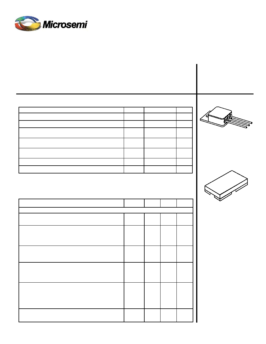
TO-254AA
U-PKG (SMD-1)
(TO-267AB)
相关PDF资料 |
PDF描述 |
|---|---|
| 2N726 | 50 mA, 20 V, PNP, Si, SMALL SIGNAL TRANSISTOR, TO-18 |
| 2N7273D | 12 A, 100 V, 0.195 ohm, N-CHANNEL, Si, POWER, MOSFET, TO-257AA |
| 2N7273H | 12 A, 100 V, 0.195 ohm, N-CHANNEL, Si, POWER, MOSFET, TO-257AA |
| 2N7274D | 8 A, 200 V, 0.5 ohm, N-CHANNEL, Si, POWER, MOSFET, TO-204AA |
| 2N7274R | 8 A, 200 V, 0.5 ohm, N-CHANNEL, Si, POWER, MOSFET, TO-204AA |
相关代理商/技术参数 |
参数描述 |
|---|---|
| 2N7236UJANTX | 制造商:International Rectifier 功能描述: |
| 2N7237 | 制造商:Microsemi Corporation 功能描述:TRANS MOSFET P-CH 11A 3PIN TO-254 - Bulk |
| 2N7241TX | 制造商:HARRIS 功能描述:2N7241TX |
| 2N726 | 制造商:CENTRAL 制造商全称:Central Semiconductor Corp 功能描述:Small Signal Transistors |
| 2N7261 | 制造商: 功能描述: 制造商:undefined 功能描述: |
发布紧急采购,3分钟左右您将得到回复。