- 您现在的位置:买卖IC网 > PDF目录30509 > 2SB1571-HX 5 A, 30 V, PNP, Si, POWER TRANSISTOR PDF资料下载
参数资料
| 型号: | 2SB1571-HX |
| 元件分类: | 功率晶体管 |
| 英文描述: | 5 A, 30 V, PNP, Si, POWER TRANSISTOR |
| 文件页数: | 1/4页 |
| 文件大小: | 41K |
| 代理商: | 2SB1571-HX |
2001
PNP SILICON EPITAXIAL TRANSISTOR
2SB1571
PNP SILICON EPITAXIAL TRANSISTOR
DATA SHEET
Document No.
D15930EJ2V0DS00 (2nd edition)
Date Published
December 2001 NS CP(K)
Printed in Japan
The information in this document is subject to change without notice. Before using this document, please
confirm that this is the latest version.
Not all devices/types available in every country. Please check with local NEC representative for
availability and additional information.
FEATURES
Low VCE(sat): VCE(sat)1 ≤ 0.35 V
Complementary to 2SD2402
ABSOLUTE MAXIMUM RATINGS (TA = 25°C)
Collector to Base Voltage
VCBO
50
V
Collector to Emitter Voltage
VCEO
30
V
Emitter to Base Voltage
VEBO
6.0
V
Collector Current (DC)
IC(DC)
5.0
A
Collector Current (pulse)
Note1
IC(pulse)
8.0
A
Base Current (DC)
IB(DC)
0.2
A
Base Current (pulse)
Note1
IB(pulse)
0.4
A
Total Power Dissipation
Note2
PT
2.0
W
Junction Temperature
Tj
150
°C
Storage Temperature Range
Tstg
–55 to + 150
°C
Notes 1. PW
≤ 10 ms, Duty Cycle ≤ 50%
2. When mounted on ceramic substrate of 16 cm
2 x 0.7 mm
ELECTRICAL CHARACTERISTICS (TA = 25°C)
CHARACTERISTICS
SYMBOL
TEST CONDITIONS
MIN.
TYP.
MAX.
UNIT
Collector Cut-off Current
ICBO
VCB =
50 V, IE = 0
100
nA
Emitter Cut-off Current
IEBO
VEB =
6.0 V, IC = 0
100
nA
DC Current Gain
Note
hFE1
VCE =
1.0 V, IC = 1.0 A
80
hFE2
VCE =
1.0 V, IC = 2.0 A
100
200
400
Base to Emitter Voltage
Note
VBE
VCE =
1.0 V, IC = 0.1 A
0.6
0.665
0.7
V
Collector Saturation Voltage
Note
VCE(sat)1
IC =
3.0 A, IB = 0.15 A
0.17
0.35
V
Collector Saturation Voltage
Note
VCE(sat)2
IC =
5.0 A, IB = 0.25 A
0.28
0.55
V
Base Saturation Voltage
Note
VBE(sat)
IC =
3.0 A, IB = 0.15 A
0.89
1.2
V
Gain Bandwidth Product
fT
VCE =
10 V, IE = 0.5 A
150
MHz
Output Capacitance
Cob
VCB =
10 V, IE = 0, f = 1.0 MHz
100
pF
Turn-on Time
ton
IC =
2.0 A, VCC = 10 V,
265
ns
Storage Time
tstg
RL = 5.0
, IB1 = IB2 = 0.1 A,
350
ns
Fall Time
tf
50
ns
Note Pulsed: PW
≤ 350
s, Duty Cycle ≤ 2%
hFE CLASSFICATION
Marking
HX
HY
HZ
hFE2
100 to 200
160 to 320
200 to 400
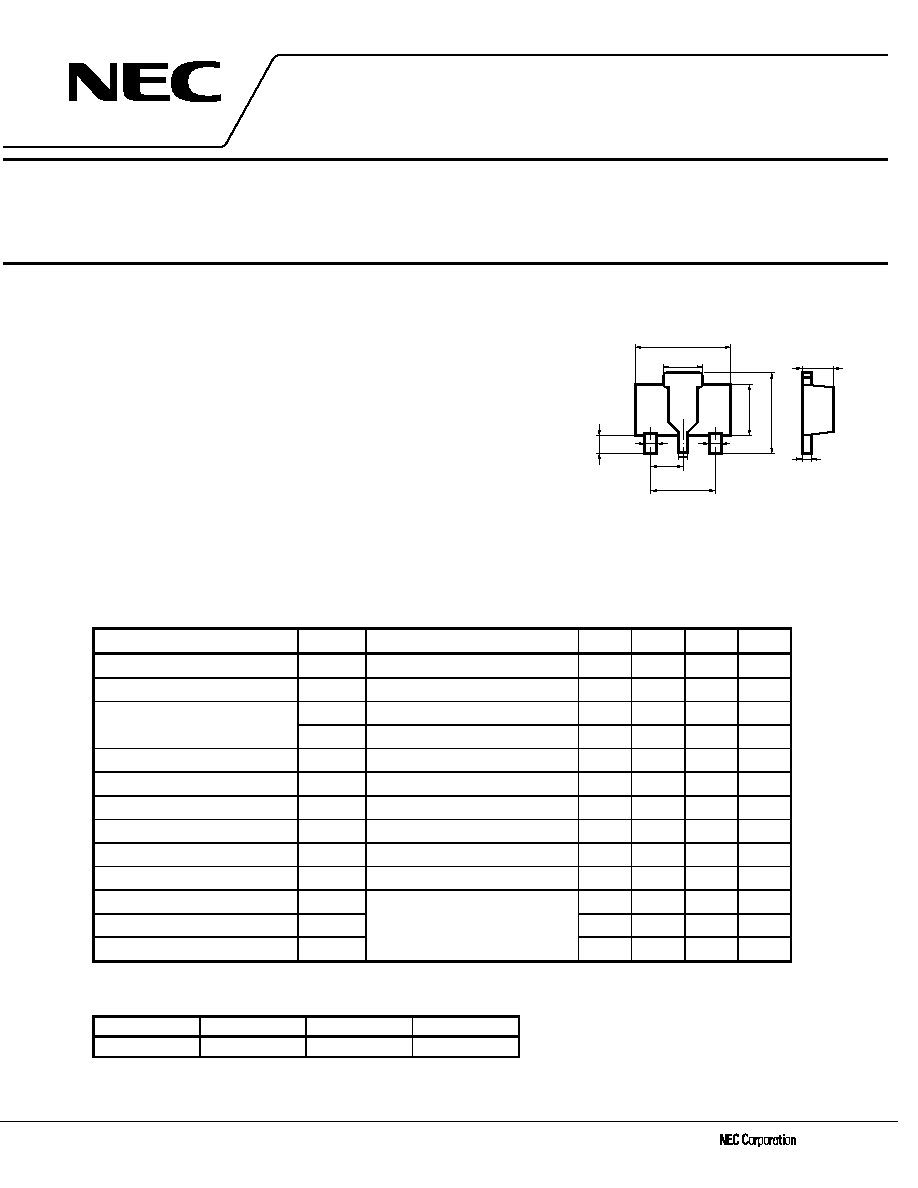
PACKAGE DRAWING (Unit: mm)
1.6±0.2
4.5±0.1
0.42
±0.06
0.8
MIN.
1.5
0.42
±0.06
0.47
±0.06
3.0
2.5±0.1
4.0±0.25
0.41
+0.03
–0.05
1.5±0.1
E
C
B
E: Emitter
C: Collector (Fin)
B: Base
相关PDF资料 |
PDF描述 |
|---|---|
| 2SB1572-HZ-AZ | 3 A, 60 V, PNP, Si, POWER TRANSISTOR |
| 2SB1572-AZ | 3 A, 60 V, PNP, Si, POWER TRANSISTOR |
| 2SB1572-HX | 3 A, 60 V, PNP, Si, POWER TRANSISTOR |
| 2SB1572-HY | 3 A, 60 V, PNP, Si, POWER TRANSISTOR |
| 2SB1572-HY-AZ | 3 A, 60 V, PNP, Si, POWER TRANSISTOR |
相关代理商/技术参数 |
参数描述 |
|---|---|
| 2SB1571-T1-AZ(FY) | 制造商:Renesas Electronics 功能描述:PNP |
| 2SB1571-T1-AZ-FZ | 制造商:Renesas Electronics Corporation 功能描述: |
| 2SB1572-T1-AZ | 制造商:Renesas Electronics 功能描述:Cut Tape 制造商:Renesas Electronics Corporation 功能描述:PNP PWR Transistor,60V,3.0A,P-MINI MOLD3 制造商:Renesas 功能描述:Trans GP BJT PNP 60V 3A 4-Pin(3+Tab) SC-62 T/R |
| 2SB1572-T1-AZ HY | 制造商:Renesas Electronics 功能描述:PNP |
| 2SB1572-T1-AZ-HZ | 制造商:Renesas Electronics Corporation 功能描述: |
发布紧急采购,3分钟左右您将得到回复。