- 您现在的位置:买卖IC网 > PDF目录41479 > 2SC2715 50 mA, 30 V, NPN, Si, SMALL SIGNAL TRANSISTOR PDF资料下载
参数资料
| 型号: | 2SC2715 |
| 元件分类: | 小信号晶体管 |
| 英文描述: | 50 mA, 30 V, NPN, Si, SMALL SIGNAL TRANSISTOR |
| 封装: | 2-3F1A, SC-59, 3 PIN |
| 文件页数: | 1/8页 |
| 文件大小: | 435K |
| 代理商: | 2SC2715 |
2SC2715
2007-11-01
1
TOSHIBA Transistor Silicon NPN Epitaxial Planar Type (PCT process)
2SC2715
High Frequency Amplifier Applications
High power gain: Gpe = 30dB (typ.) (f = 10.7 MHz)
Recommended for FM IF, OSC stage and AM CONV. IF stage.
Absolute Maximum Ratings (Ta = 25°C)
Characteristics
Symbol
Rating
Unit
Collector-base voltage
VCBO
35
V
Collector-emitter voltage
VCEO
30
V
Emitter-base voltage
VEBO
4
V
Collector current
IC
50
mA
Base current
IB
10
mA
Collector power dissipation
PC
150
mW
Junction temperature
Tj
125
°C
Storage temperature range
Tstg
55~125
°C
Note: Using continuously under heavy loads (e.g. the application of high
temperature/current/voltage and the significant change in
temperature, etc.) may cause this product to decrease in the
reliability significantly even if the operating conditions (i.e.
operating temperature/current/voltage, etc.) are within the
absolute maximum ratings.
Please design the appropriate reliability upon reviewing the Toshiba Semiconductor Reliability Handbook
(“Handling Precautions”/“Derating Concept and Methods”) and individual reliability data (i.e. reliability test
report and estimated failure rate, etc).
Electrical Characteristics (Ta = 25°C)
Characteristics
Symbol
Test Condition
Min
Typ.
Max
Unit
Collector cut-off current
ICBO
VCB = 35 V, IE = 0
0.1
μA
Emitter cut-off current
IEBO
VEB = 4 V, IC = 0
1.0
μA
DC current gain
hFE
(Note)
VCE = 12 V, IC = 2 mA
40
240
Collector-emitter saturation voltage
VCE (sat)
IC = 10 mA, IB = 1 mA
0.4
V
Base-emitter voltage
VBE
IC = 10 mA, IB = 1 mA
1.0
V
Transition frequency
fT
VCE = 10 V, IC = 1 mA
100
400
MHz
Collector output capacitance
Cob
VCB = 10 V, IE = 0, f = 1 MHz
2.0
3.2
pF
Collector-base time constant
Ccrbb’
VCE = 10 V, IE = 1 mA, f = 30 MHz
50
ps
Power gain
Gpe
VCC = 6 V, IE = 1 mA, f = 10.7 MHz
(Figure 1)
27
30
33
dB
Note: hFE classification R: 40~80, O: 70~140, Y: 120~240
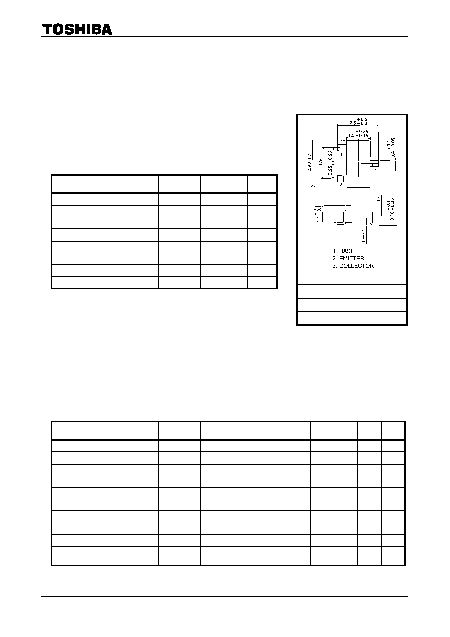
Unit: mm
JEDEC
―
JEITA
SC-59
TOSHIBA
2-3F1A
Weight: 0.012 g (typ.)
USM
相关PDF资料 |
PDF描述 |
|---|---|
| 2SC2715-O | 50 mA, 30 V, NPN, Si, SMALL SIGNAL TRANSISTOR |
| 2SC2734 | UHF BAND, Si, NPN, RF SMALL SIGNAL TRANSISTOR |
| 2SC2734 | UHF BAND, Si, NPN, RF SMALL SIGNAL TRANSISTOR |
| 2SC2736 | UHF BAND, Si, NPN, RF SMALL SIGNAL TRANSISTOR |
| 2SC2880OTE12R | 50 mA, 150 V, NPN, Si, SMALL SIGNAL TRANSISTOR |
相关代理商/技术参数 |
参数描述 |
|---|---|
| 2SC2715-O(TE85L,F) | 制造商:Toshiba 功能描述:NPN |
| 2SC2716 | 制造商:Distributed By MCM 功能描述:SUB ONLY TOSHIBA TRANS. SC-5935V .1A .15W ECB SURFACE MOUNT |
| 2SC2716-Y(TE85L,F) | 制造商:Toshiba 功能描述:NPN |
| 2SC2717 | 制造商:Distributed By MCM 功能描述:SUB ONLY TOSHIBA TRANS. TO-9230V .05A .3W BEC |
| 2SC2717(F) | 制造商:Toshiba 功能描述:NPN Cut Tape |
发布紧急采购,3分钟左右您将得到回复。