- 您现在的位置:买卖IC网 > PDF目录141202 > 2SC2958-M 500 mA, 140 V, NPN, Si, SMALL SIGNAL TRANSISTOR PDF资料下载
参数资料
| 型号: | 2SC2958-M |
| 元件分类: | 小信号晶体管 |
| 英文描述: | 500 mA, 140 V, NPN, Si, SMALL SIGNAL TRANSISTOR |
| 文件页数: | 3/4页 |
| 文件大小: | 198K |
| 代理商: | 2SC2958-M |
1998
Document No. D16150EJ1V0DS00
Date Published April 2002 N CP(K)
Printed in Japan
SILICON TRANSISTORS
2SC2958, 2959
NPN SILICON EPITAXIAL TRANSISTOR
FOR LOW-FREQUENCY POWER AMPLIFIERS
DATA SHEET
2002
The information in this document is subject to change without notice. Before using this document, please
confirm that this is the latest version.
Not all devices/types available in every country. Please check with local NEC representative for
availability and additional information.
FEATURES
Ideal for use of high voltage current such as TV vertical
deflection (drive and output), audio output, pin cushion
correction
Complementary transistor with 2SA1221 and 2SA1222
VCEO = 140 V: 2SA1221/2SC2958
VCEO = 160 V: 2SA1222/2SC2959
ABSOLUTE MAXIMUM RATINGS (Ta = 25
°°°°C)
Parameter
Symbol
Ratings
Unit
Collector to base voltage
VCBO
160
V
Collector to emitter voltage
VCEO
140/160
V
Emitter to base voltage
VEBO
5.0
V
Collector current (DC)
IC(DC)
500
mA
Collector current (pulse)
IC(pulse)*1.0
A
Total power dissipation
PT
1.0
W
Junction temperature
Tj
150
°C
Storage temperature
Tstg
55 to +150
°C
*PW
≤ 10 ms, duty cycle ≤ 50%
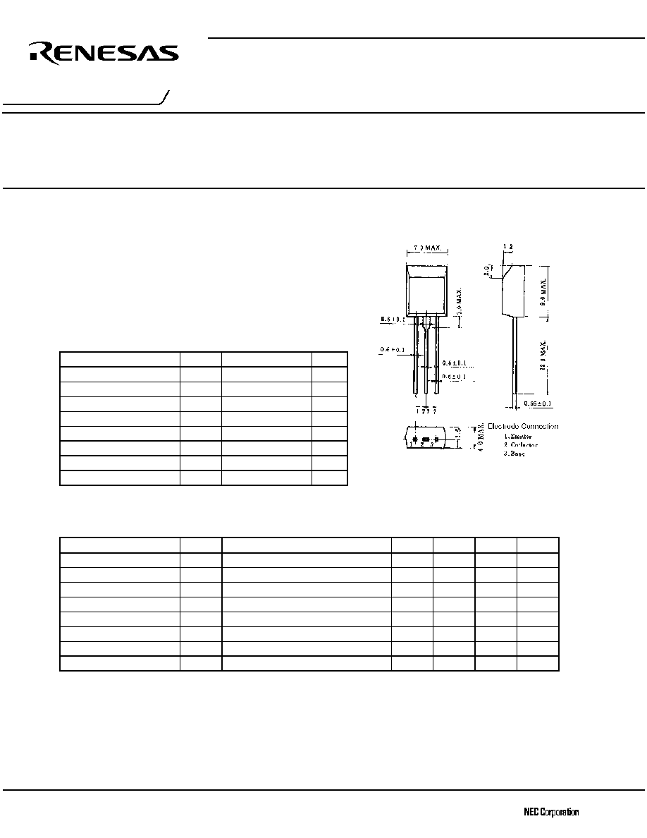
PACKAGE DRAWING (UNIT: mm)
ELECTRICAL CHARACTERISTICS (Ta = 25
°°°°C)
Parameter
Symbol
Conditions
MIN.
TYP.
MAX.
Unit
Collector cutoff current
ICBO
VCB = 100 V, IE = 0
200
nA
Emitter cutoff current
IEBO
VEB = 5.0 V, IC = 0
200
nA
DC current gain
hFE **
VCE = 2.0 V, IC = 100 mA
100
150
400
DC base voltage
VBE **
VCE = 5.0 V, IC = 20 mA
0.6
0.64
0.7
V
Collector saturation voltage
VCE(sat) **
IC = 1.0 A, IB = 0.2 A
0.32
0.7
V
Base saturation voltage
VBE(sat) **
IC = 1.0 A, IB = 0.2 A
1.1
1.3
V
Output capacitance
Cob
VCB = 10 V, IE = 0, f = 1.0 MHz
13
30
pF
Gain bandwidth product
fT
VCE = 10 V, IE =
20 mA
30
60
MHz
** Pulse test PW
≤ 350
s, duty cycle ≤ 2% per pulsed
相关PDF资料 |
PDF描述 |
|---|---|
| 2SC2959-M | 500 mA, 160 V, NPN, Si, SMALL SIGNAL TRANSISTOR |
| 2SC3360-N15 | 100 mA, 200 V, NPN, Si, SMALL SIGNAL TRANSISTOR |
| 2SC3623A | 150 mA, 50 V, NPN, Si, SMALL SIGNAL TRANSISTOR |
| 2SC4331M | 5000 mA, 100 V, NPN, Si, SMALL SIGNAL TRANSISTOR, TO-251AA |
| 2SC4332-ZM | 5000 mA, 60 V, NPN, Si, SMALL SIGNAL TRANSISTOR |
相关代理商/技术参数 |
参数描述 |
|---|---|
| 2SC2959 | 制造商:Distributed By MCM 功能描述:SUB ONLY NEC TRANSISTOR SP-8 160V .5A 1W ECB |
| 2SC2959K | 制造商:Renesas Electronics 功能描述:NPN 制造商:Renesas Electronics 功能描述:NPN Bulk |
| 2SC2959-K-AZ | 制造商:Renesas Electronics Corporation 功能描述: |
| 2SC2960 | 制造商:Distributed By MCM 功能描述:SUB ONLY SANYO TRANSISTOR SPA60V .15A .25W |
| 2SC2979 | 制造商:Hitachi 功能描述:TRANSISTOR NPN TO-220 |
发布紧急采购,3分钟左右您将得到回复。