参数资料
| 型号: | 34VL02/P |
| 厂商: | Microchip Technology |
| 文件页数: | 7/32页 |
| 文件大小: | 0K |
| 描述: | IC EEPROM 2KBIT 400KHZ 8DIP |
| 产品培训模块: | I2C Serial EEPROM |
| 标准包装: | 60 |
| 格式 - 存储器: | EEPROMs - 串行 |
| 存储器类型: | EEPROM |
| 存储容量: | 2K (256 x 8) |
| 速度: | 400kHz |
| 接口: | I²C,2 线串口 |
| 电源电压: | 1.5 V ~ 3.6 V |
| 工作温度: | 0°C ~ 70°C |
| 封装/外壳: | 8-DIP(0.300",7.62mm) |
| 供应商设备封装: | 8-PDIP |
| 包装: | 管件 |
第1页第2页第3页第4页第5页第6页当前第7页第8页第9页第10页第11页第12页第13页第14页第15页第16页第17页第18页第19页第20页第21页第22页第23页第24页第25页第26页第27页第28页第29页第30页第31页第32页
�� �
�
�34VL02�
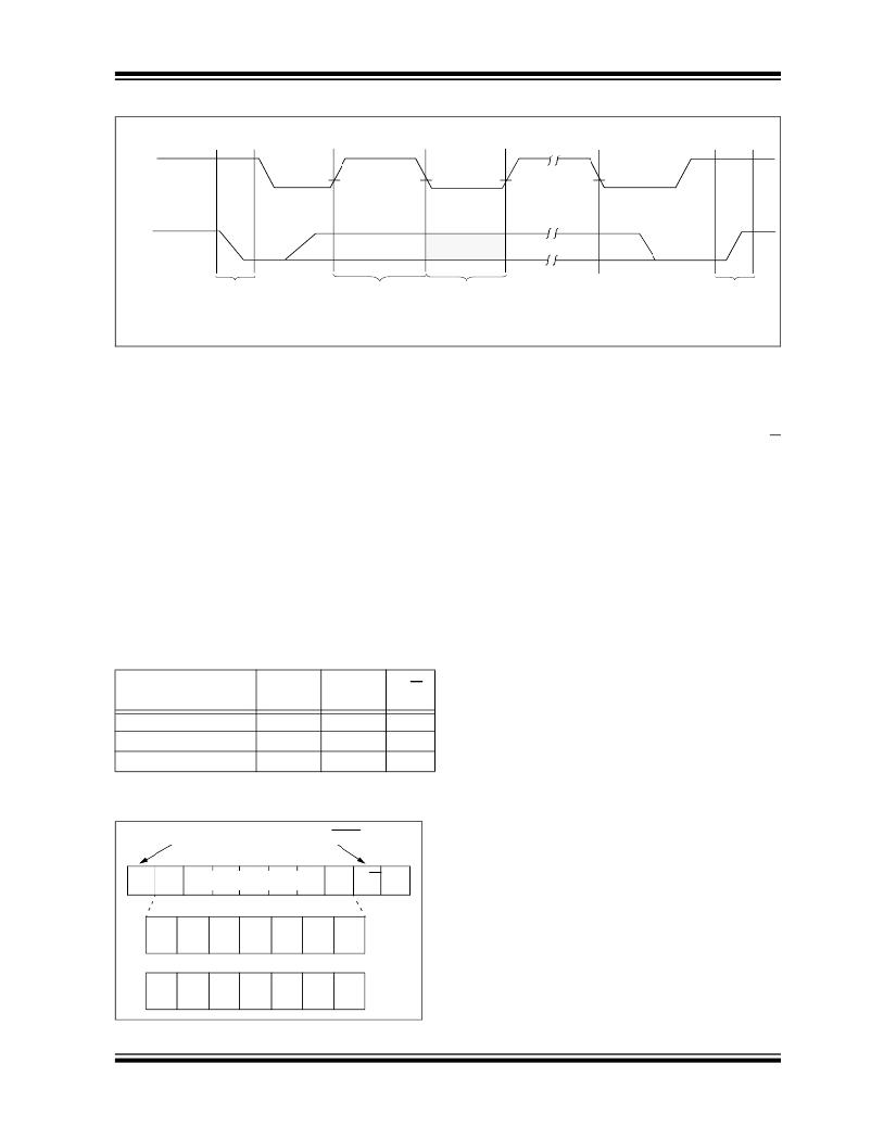
�FIGURE� 3-1:�
�DATA� TRANSFER� SEQUENCE� ON� THE� SERIAL� BUS�
�SCL�
�(A)�
�(B)�
�(D)�
�(D)�
�(C)�
�(A)�
�SDA�
�Start�
�Condition�
�Address� or�
�Acknowledge�
�Valid�
�Data�
�Allowed�
�to� Change�
�Stop�
�Condition�
�3.6�
�Device� Addressing�
�4.0�
�WRITE� OPERATIONS�
�A� control� byte� is� the� first� byte� received� following� the�
�Start� condition� from� the� master� device.� The� first� part� of�
�4.1�
�Byte� Write�
�the� control� byte� consists� of� a� 4-bit� control� code� which� is�
�set� to� ‘� 1010� ’� for� normal� read� and� write� operations� and�
�‘� 0110� ’� for� writing� to� the� write-protect� register.� The�
�control� byte� is� followed� by� three� Chip� Select� bits� (A2,�
�A1,� A0).� The� Chip� Select� bits� allow� the� use� of� up� to�
�eight� 34VL02� devices� on� the� same� bus� and� are� used� to�
�determine� which� device� is� accessed.� The� Chip� Select�
�bits� in� the� control� byte� must� correspond� to� the� logic� lev-�
�els� on� the� corresponding� A2,� A1� and� A0� pins� for� the�
�device� to� respond.�
�The� eighth� bit� of� slave� address� determines� if� the� master�
�device� wants� to� read� or� write� to� the� 34VL02�
�(Figure� 3-2).� When� set� to� a� one,� a� read� operation� is�
�selected.� When� set� to� a� zero,� a� write� operation� is�
�selected.�
�Following� the� Start� signal� from� the� master,� the� device�
�code(4� bits),� the� Chip� Select� bits� (3� bits)� and� the� R/W�
�bit,� which� is� a� logic� low,� are� placed� onto� the� bus� by� the�
�master� transmitter.� This� indicates� to� the� addressed�
�slave� receiver� that� a� byte� with� a� word� address� will� follow,�
�once� it� has� generated� an� Acknowledge� bit� during� the�
�ninth� clock� cycle.� Therefore,� the� next� byte� transmitted�
�by� the� master� is� the� word� address� and� will� be� written�
�into� the� Address� Pointer� of� the� 34VL02.�
�After� receiving� another� Acknowledge� signal� from� the�
�34VL02,� the� master� device� will� transmit� the� data� word� to�
�be� written� into� the� addressed� memory� location.� The�
�34VL02� acknowledges� again� and� the� master� generates�
�a� Stop� condition.� This� initiates� the� internal� write� cycle,�
�which� means� that� during� this� time,� the� 34VL02� will� not�
�generate� Acknowledge� signals� (Figure� 4-1).� If� an�
�Read�
�Write�
�Operation�
�Control�
�Code�
�1010�
�1010�
�Chip�
�Select�
�A2� A1� A0�
�A2� A1� A0�
�R/W�
�1�
�0�
�attempt� is� made� to� write� to� the� array� when� the� software�
�or� hardware� write� protection� has� been� enabled,� the�
�device� will� acknowledge� the� command,� but� no� data� will�
�be� written.� The� write� cycle� time� must� be� observed� even�
�if� the� write� protection� is� enabled.�
�Write-Protect� Register�
�0110�
�A2� A1� A0�
�0�
�4.2�
�Page� Write�
�FIGURE� 3-2:�
�Start�
�CONTROL� BYTE�
�ALLOCATION�
�Read/Write�
�The� write� control� byte,� word� address� and� the� first� data�
�byte� are� transmitted� to� the� 34VL02� in� the� same� way� as�
�in� a� byte� write.� Instead� of� generating� a� Stop� condition,�
�the� master� transmits� up� to� 15� additional� data� bytes� to�
�the� 34VL02,� which� are� temporarily� stored� in� the� on-chip�
�Slave� Address�
�R/W� A�
�page� buffer� and� will� be� written� into� the� memory� after� the�
�master� has� transmitted� a� Stop� condition.� Upon� receipt�
�of� each� word,� the� four� lower� order� Address� Pointer� bits�
�1�
�0�
�1�
�0�
�A2�
�A1�
�A0�
�are� internally� incremented� by� one.� The� higher� order�
�four� bits� of� the� word� address� remain� constant.� If� the�
�OR�
�master� should� transmit� more� than� 16� bytes� prior� to� gen-�
�erating� the� Stop� condition,� the� address� counter� will� roll�
�0�
�1�
�1�
�0�
�A2�
�A1�
�A0�
�over� and� the� previously� received� data� will� be� overwrit-�
�ten.� As� with� the� byte� write� operation,� once� the� Stop�
�condition� is� received,� an� internal� write� cycle� will� begin�
�?� 2008� Microchip� Technology� Inc.�
�DS22079A-page� 7�
�相关PDF资料 |
PDF描述 |
|---|---|
| XC6SLX9-2CSG324I | IC FPAG SPARTAN 6 9K 324CSGBGA |
| XA3S400-4FTG256I | IC FPGA SPARTAN-3 400K 256-FTBGA |
| XC3S400A-4FG320I | IC SPARTAN-3A FPGA 400K 320FBGA |
| XC3S400A-4FGG320I | IC SPARTAN-3A FPGA 400K 320FBGA |
| XC3S250E-4PQ208I | IC FPGA SPARTAN 3E 208PQFP |
相关代理商/技术参数 |
参数描述 |
|---|---|
| 34VL02T/MNY | 功能描述:电可擦除可编程只读存储器 2K 256X8 1.5V SERIAL EE RoHS:否 制造商:Atmel 存储容量:2 Kbit 组织:256 B x 8 数据保留:100 yr 最大时钟频率:1000 KHz 最大工作电流:6 uA 工作电源电压:1.7 V to 5.5 V 最大工作温度:+ 85 C 安装风格:SMD/SMT 封装 / 箱体:SOIC-8 |
| 34VL02T/MS | 功能描述:电可擦除可编程只读存储器 2K 256X8 1.5V SERIAL EE RoHS:否 制造商:Atmel 存储容量:2 Kbit 组织:256 B x 8 数据保留:100 yr 最大时钟频率:1000 KHz 最大工作电流:6 uA 工作电源电压:1.7 V to 5.5 V 最大工作温度:+ 85 C 安装风格:SMD/SMT 封装 / 箱体:SOIC-8 |
| 34VL02T/OT | 功能描述:电可擦除可编程只读存储器 2K 256X8 1.5V SERIAL EE RoHS:否 制造商:Atmel 存储容量:2 Kbit 组织:256 B x 8 数据保留:100 yr 最大时钟频率:1000 KHz 最大工作电流:6 uA 工作电源电压:1.7 V to 5.5 V 最大工作温度:+ 85 C 安装风格:SMD/SMT 封装 / 箱体:SOIC-8 |
| 34VL02T/SN | 功能描述:电可擦除可编程只读存储器 2K 256X8 1.5V SERIAL EE RoHS:否 制造商:Atmel 存储容量:2 Kbit 组织:256 B x 8 数据保留:100 yr 最大时钟频率:1000 KHz 最大工作电流:6 uA 工作电源电压:1.7 V to 5.5 V 最大工作温度:+ 85 C 安装风格:SMD/SMT 封装 / 箱体:SOIC-8 |
| 34VL02T/ST | 功能描述:电可擦除可编程只读存储器 2K 256X8 1.5V RoHS:否 制造商:Atmel 存储容量:2 Kbit 组织:256 B x 8 数据保留:100 yr 最大时钟频率:1000 KHz 最大工作电流:6 uA 工作电源电压:1.7 V to 5.5 V 最大工作温度:+ 85 C 安装风格:SMD/SMT 封装 / 箱体:SOIC-8 |
发布紧急采购,3分钟左右您将得到回复。