- 您现在的位置:买卖IC网 > PDF目录293797 > 3584JM High Voltage, High Speed OPERATIONAL AMPLIFIER PDF资料下载
参数资料
| 型号: | 3584JM |
| 元件分类: | 运算放大器 |
| 英文描述: | High Voltage, High Speed OPERATIONAL AMPLIFIER |
| 中文描述: | 高压,高速运算放大器 |
| 文件页数: | 5/6页 |
| 文件大小: | 52K |
| 代理商: | 3584JM |
3584
5
TYPICAL PERFORMANCE CURVES (CONT)
TCASE = +25°C, VS = ±150V, unless otherwise noted.
APPLICATION INFORMATION
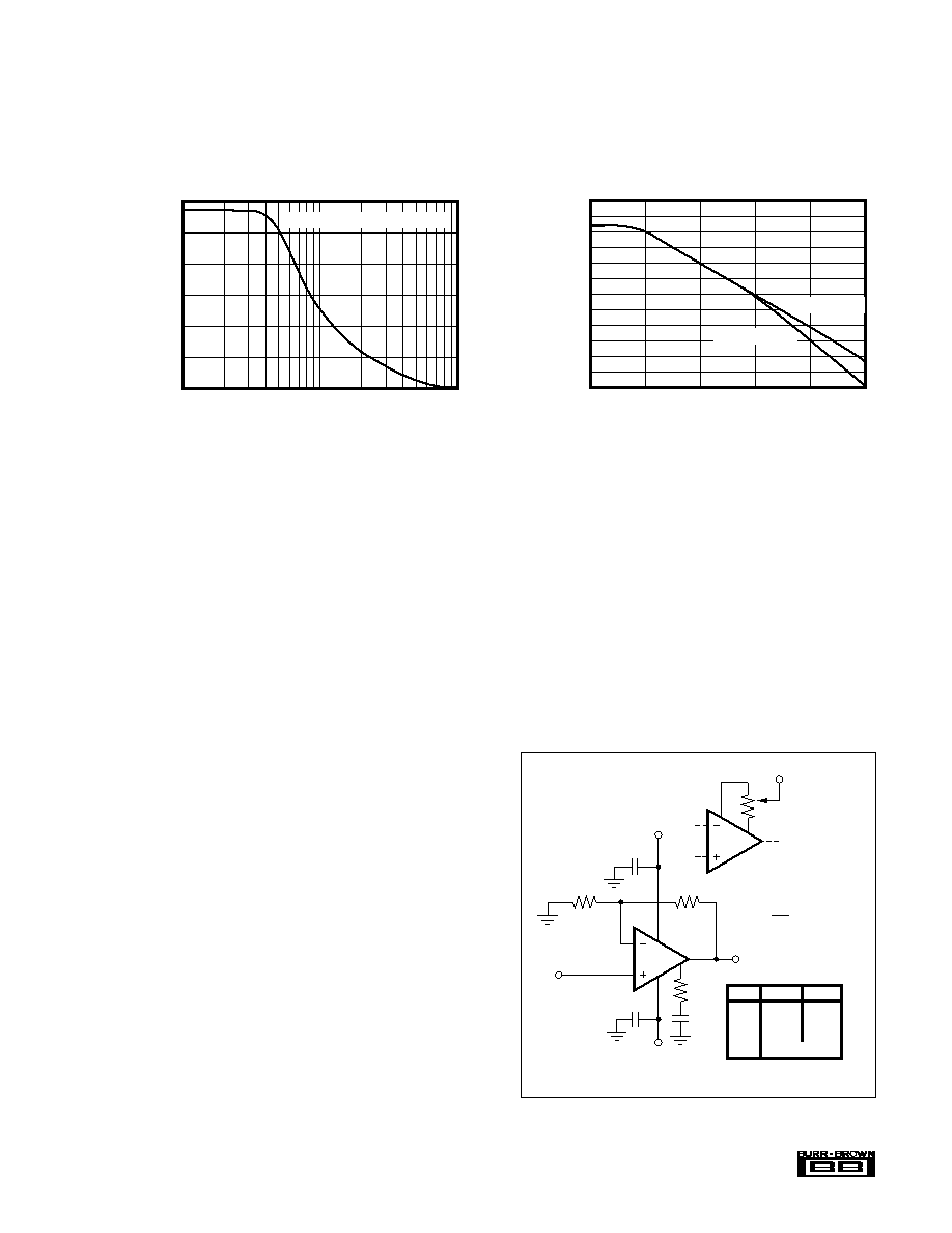
Figure 1 shows the basic connections required to operate the
3584. Bypass capacitors should be connected close to the
device pins. Be sure that these capacitors have an adequate
voltage rating.
Frequency compensation components must be connected to
pin 8 for closed-loop gains of 100 or less. Recommended
values are shown in Figure 1. Some adjustment in these
values may be required depending on exact circuit configu-
ration and load conditions. Be sure the compensation capaci-
tor has a voltage rating equal to or greater than the positive
power supply voltage, V+. Standard 0.25W resistors can be
used for R
C.
Input offset voltage and drift of the 3584 are laser-trimmed.
Many applications require no external offset trimming.
Figure 1 shows connection of an optional offset trim poten-
tiometer which connects to pins 3 and 4.
FET input circuitry reduces the input bias current of the
3584 to less than 20pA at room temperature. Input bias
current remains nearly constant throughout the full com-
mon-mode range. Input bias current approximately doubles
for each 10
°C increase in case temperature above 25°C.
Heat sinking can help minimize this effect by reducing the
case temperature.
Input circuitry of the 3584 is protected with series limiting
resistors and input clamp diodes. The inputs can withstand
the full rated supply voltage of
±150V (common-mode or
differential).
THERMAL PROTECTION
The 3584 has internal thermal shut-down circuitry that
activates at a case temperature of approximately 150
°C or
higher. As this circuitry is activated, the output current drive
is reduced. As the case temperature returns to less than the
activation temperature, operation will return to normal.
The thermal shut-down circuit will normally protect the
amplifier during a short-circuit to ground. It will not protect
against short-circuit to one of the power supplies. The
typical performance curve “Safe Operating Area” shows that
the large stress occurring during this high voltage condition
may cause damage if it exceeds 5ms duration. The thermal
protection circuitry will not activate fast enough to protect
the device from short-circuits to one of the power supplies.
The package case of the 3584 is electrically isolated from all
circuitry. No special insulating hardware is required. Al-
though not absolutely required, it is recommended that the
case be connected to ground.
FIGURE 1. Basic Circuit Connections.
3584
0.1F
V+
–70V to –150V
R
2
R
1
V
O
G = 1 +
R
2
R
1
Connect case
to ground.
V–
+70V to +150V
3
4
100k
V+
Optional offset
voltage trim
circuit.
V
IN
5
6
2
1
7
8
R
C
3584
Gain
C
R
C
1
10nF
200
10
500pF
2k
100
50pF
20k
1000
(no connection)
Interpolate values for
intermediate gains.
0
MAXIMUM COMMON-MODE VOLTAGE
vs FREQUENCY
100k
10k
1M
Common-Mode
Voltage
(±)
150
125
100
75
50
25
Frequency (Hz)
Compensation: 200
and 0.01F
10
Frequency (Hz)
0
POWER SUPPLY REJECTION vsFREQUENCY
Power
Supply
Rejection
(dB)
120
100
80
60
40
20
100
1k
10k
100k
1M
Negative Supply
Positive Supply
相关PDF资料 |
PDF描述 |
|---|---|
| 3584 | High Voltage, High Speed OPERATIONAL AMPLIFIER |
| 35863-1127 | 11 CONTACT(S), FEMALE, RIGHT ANGLE FFC/FPC CONNECTOR, SURFACE MOUNT |
| 35863-1227 | 12 CONTACT(S), FEMALE, RIGHT ANGLE FFC/FPC CONNECTOR, SURFACE MOUNT |
| 35863-1327 | 13 CONTACT(S), FEMALE, RIGHT ANGLE FFC/FPC CONNECTOR, SURFACE MOUNT |
| 35863-1627 | 16 CONTACT(S), FEMALE, RIGHT ANGLE FFC/FPC CONNECTOR, SURFACE MOUNT |
相关代理商/技术参数 |
参数描述 |
|---|---|
| 3585 | 制造商:SPC Multicomp 功能描述:Basic Electronic Tool Kit 22 Pcs inclu 制造商:VISUAL COMMUNICATIONS COMPANY LLC 功能描述:3585 /Custom Part |
| 3585/25 | 制造商:Alpha Wire Company 功能描述:Round & flat 25 way ribbon cable,30m |
| 3585/25 BK005 | 功能描述:扁平电缆 28AWG 25C UNSHLD 100ft SPOOL BLACK RoHS:否 制造商:3M Electronic Solutions Division 产品:Ribbon Cable 导体数量:10 导体间隔:0.5 mm 绞合:19 x 40 线规 - 美国线规(AWG):28 电压额定值:300 V 屏蔽:Unshielded 导体材料:Copper Alloy 外壳材料:Halogen Free Polyolefin (PO) 颜色:Dark Gray 工作温度范围:- 40 C to + 105 C 电缆类型:Flat Cable 绝缘材料: |
| 3585/25-BK005 | 制造商:Alpha Wire Company 功能描述:Round Flat Cable 25Conductors 28AWG 8.64mm Tinned Copper Gray 300VAC |
| 3585/25-BLACK-100 | 制造商:Alpha Wire Company 功能描述:Round Flat Cable 25Conductors 28AWG 8.64mm Tinned Copper Black 300V |
发布紧急采购,3分钟左右您将得到回复。