- 您现在的位置:买卖IC网 > PDF目录298320 > 3D7424D-1 (DATA DELAY DEVICES INC) MONOLITHIC QUAD 4-BIT PROGRAMMABLE DELAY LINE PDF资料下载
参数资料
| 型号: | 3D7424D-1 |
| 厂商: | DATA DELAY DEVICES INC |
| 元件分类: | 延迟线 |
| 英文描述: | MONOLITHIC QUAD 4-BIT PROGRAMMABLE DELAY LINE |
| 中文描述: | ACTIVE DELAY LINE, TRUE OUTPUT, PDSO14 |
| 封装: | ROHS COMPLIANT, SOIC-14 |
| 文件页数: | 2/6页 |
| 文件大小: | 392K |
| 代理商: | 3D7424D-1 |
3D7424
APPLICATION NOTES
THEORY OF OPERATION
PROGRAMMED DELAY INTERFACE
The quad 4-bit programmable 3D7424 device
architecture is comprised of four independently
operating delay lines. Each delay line produces
at its output a replica of the signal present at its
input, shifted in time. A single delay line is
comprised of a number of delay cells connected
in series. Delay selection is achieved by routing
one output in each string of cells to its respective
output pin (O1-O4). The delay of each of the four
lines can be controlled independently, via the
serial interface, as described in the next section.
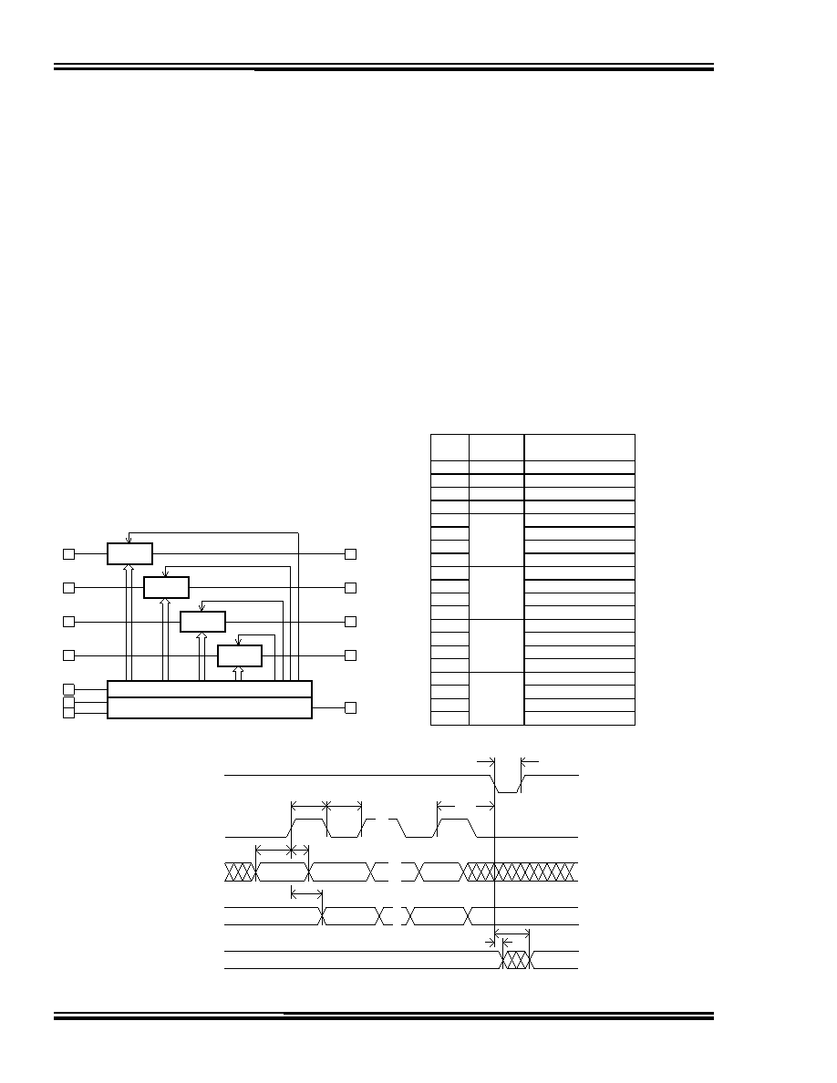
Figure 1 illustrates the main functional blocks of
the 3D7424 device. Since the device is a CMOS
design, all unused input pins must be returned to
well defined logic levels (VDD or GND). The
delays are adjusted by first shifting a 20-bit
programming word into the device via the SC and
SI pins, then strobing the AL signal to latch the
values. The bit sequence is shown in Table 2,
and the associated timing diagram is shown in
Figure 2. Each line has associated with it an
enable bit. Setting this bit low will force the
corresponding delay line output to a high
impedance state, while setting it high returns the
The change in delay from one address setting to
the next is called the increment, or LSB. It is
nominally equal to the device dash number. The
minimum delay, achieved by setting the address
of a line to zero, is called the inherent delay.
line to its normal operation. The device contains
an SO output, which can be used to cascade
multiple devices, as shown in Figure 3.
TABLE 2: BIT SEQUENCE
For best performance, it is essential that the
power supply pin be adequately bypassed and
filtered. In addition, the power bus should be of
as low an impedance construction as possible.
Power planes are preferred. Also, signal traces
should be kept as short as possible.
Bit
Delay
Line
Function
1
4
Output Enable
2
3
Output Enable
3
2
Output Enable
4
1
Output Enable
5
Address Bit 3
6
Address Bit 2
7
Address Bit 1
8
1
Address Bit 0
9
Address Bit 3
10
Address Bit 2
11
Address Bit 1
12
2
Address Bit 0
13
Address Bit 3
14
Address Bit 2
15
Address Bit 1
16
3
Address Bit 0
17
Address Bit 3
18
Address Bit 2
19
Address Bit 1
20
4
Address Bit 0
DELAY
LINE
20-BIT LATCH
20-BIT SHIFT REGISTER
SO
Figure 1: Functional block diagram
DELAY
LINE
DELAY
LINE
DELAY
LINE
I4
I3
I2
I1
O4
O3
O2
O1
AL
SI
SC
ENABLES
ADDR4
ADDR3
ADDR2
ADDR1
NEW
VALUES
NEW
BIT 1
NEW
BIT 20
NEW
BIT 2
OLD
BIT 1
OLD
BIT 2
OLD
BIT 20
LATCH
(AL)
CLOCK
(SC)
SERIAL
INPUT
(SI)
SERIAL
OUTPUT
(SO)
DELAY
TIMES
tLW
tCW
tCSL
tDSC
tDHC
tPCQ
tLDV
tLDX
PREVIOUS VALUES
Figure 2: Serial interface timing diagram
NEW
BIT 1
Doc #06019
DATA DELAY DEVICES, INC.
2
6/25/2007
Tel: 973-773-2299
Fax: 973-773-9672
http://www.datadelay.com
相关PDF资料 |
PDF描述 |
|---|---|
| 3D7424D-1.5 | MONOLITHIC QUAD 4-BIT PROGRAMMABLE DELAY LINE |
| 3D7424D-10 | MONOLITHIC QUAD 4-BIT PROGRAMMABLE DELAY LINE |
| 3D7424D-100 | MONOLITHIC QUAD 4-BIT PROGRAMMABLE DELAY LINE |
| 3D7424D-15 | MONOLITHIC QUAD 4-BIT PROGRAMMABLE DELAY LINE |
| 3D7424 | MONOLITHIC QUAD 4-BIT PROGRAMMABLE DELAY LINE |
相关代理商/技术参数 |
参数描述 |
|---|---|
| 3D7424D-1.5 | 制造商:DATADELAY 制造商全称:Data Delay Devices, Inc. 功能描述:MONOLITHIC QUAD 4-BIT PROGRAMMABLE DELAY LINE |
| 3D7424D-10 | 制造商:DATADELAY 制造商全称:Data Delay Devices, Inc. 功能描述:MONOLITHIC QUAD 4-BIT PROGRAMMABLE DELAY LINE |
| 3D7424D-100 | 制造商:DATADELAY 制造商全称:Data Delay Devices, Inc. 功能描述:MONOLITHIC QUAD 4-BIT PROGRAMMABLE DELAY LINE |
| 3D7424D-15 | 制造商:DATADELAY 制造商全称:Data Delay Devices, Inc. 功能描述:MONOLITHIC QUAD 4-BIT PROGRAMMABLE DELAY LINE |
| 3D7424D-2 | 制造商:DATADELAY 制造商全称:Data Delay Devices, Inc. 功能描述:MONOLITHIC QUAD 4-BIT PROGRAMMABLE DELAY LINE |
发布紧急采购,3分钟左右您将得到回复。