- 您现在的位置:买卖IC网 > PDF目录298320 > 3D7428Z-4 (DATA DELAY DEVICES INC) MONOLITHIC 8-BIT PROGRAMMABLE DELAY LINE PDF资料下载
参数资料
| 型号: | 3D7428Z-4 |
| 厂商: | DATA DELAY DEVICES INC |
| 元件分类: | 延迟线 |
| 英文描述: | MONOLITHIC 8-BIT PROGRAMMABLE DELAY LINE |
| 中文描述: | SILICON DELAY LINE, TRUE OUTPUT, PDSO8 |
| 封装: | SOIC-8 |
| 文件页数: | 4/7页 |
| 文件大小: | 514K |
| 代理商: | 3D7428Z-4 |
3D7428
APPLICATION NOTES (CONT’D)
LATCHED PARALLEL MODE
(MD = 1, AE PULSED)
The eight program pins P0 - P7 are loaded by the
falling edge of the Enable pulse, as shown in
Figure 3. After each change in delay value, a
settling time tEDV is required before the input is
accurately delayed.
SERIAL MODE (MD = 0)
While observing data setup (tDSC) and data hold
(tDHC) requirements, timing data is loaded in
MSB-to-LSB order by the rising edge of the clock
(SC) while the enable (AE) is high, as shown in
Figure 4. The falling edge of the enable (AE)
activates the new delay value which is reflected
at the output after a settling time tEDV. As data is
shifted into the serial data input (SI), the previous
contents of the 8-bit input register are shifted out
of the serial output port pin (SO) in MSB-to-LSB
order, thus allowing cascading of multiple
devices by connecting the serial output pin (SO)
of the preceding device to the serial data input
pin (SI) of the succeeding device, as illustrated in
Figure 5. The total number of serial data bits in a
cascade configuration must be eight times the
number of units, and each group of eight bits
must be transmitted in MSB-to-LSB order.
To initiate a serial read, enable (AE) is driven
high. After a time tEQV , bit 7 (MSB) is valid at the
serial output port pin (SO). On the first rising
edge of the serial clock (SC), bit 7 is loaded with
the value present at the serial data input pin (SI),
while bit 6 is presented at the serial output pin
(SO). To retrieve the remaining bits seven more
rising edges must be generated on the serial
clock line. The read operation is destructive.
Therefore, if it is desired that the original delay
setting remain unchanged, the read data must be
written back to the device(s) before the enable
(AE) pin is brought low.
The SO pin, if unused, must be allowed to float if
the device is configured in the serial
programming mode.
The serial mode is the only mode available on
the 8-pin version of the 3D7428.
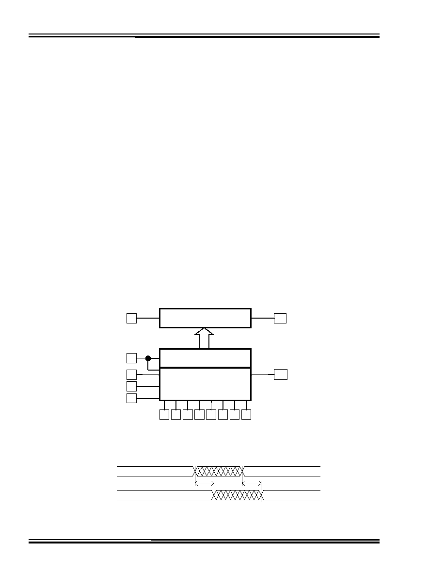
PROGRAMMABLE
DELAY LINE
LATCH
8-BIT INPUT
REGISTER
MD
SC
SI
AE
IN
SO
OUT
P0 P1 P2 P3 P4 P5 P6 P7
MODE SELECT
SHIFT CLOCK
SERIAL INPUT
ADDRESS ENABLE
SIGNAL IN
SIGNAL OUT
SERIAL OUTPUT
PARALLEL INPUTS
Figure1: Functional block diagram
PREVIOUS
NEW VALUE
tPDX
tPDV
PARALLEL
INPUTS
P0-P7
DELAY
TIME
Figure 2: Non-latched parallel mode (MD=1, AE=1)
Doc #03003
DATA DELAY DEVICES, INC.
4
5/8/2006
Tel: 973-773-2299
Fax: 973-773-9672
http://www.datadelay.com
相关PDF资料 |
PDF描述 |
|---|---|
| 3D7428Z-5 | MONOLITHIC 8-BIT PROGRAMMABLE DELAY LINE |
| 3D7428Z-7.5 | MONOLITHIC 8-BIT PROGRAMMABLE DELAY LINE |
| 3D7523-0.5 | MONOLITHIC MANCHESTER ENCODER/DECODER |
| 3D7523 | MONOLITHIC MANCHESTER ENCODER/DECODER |
| 3EZ120D5 | surface mount silicon Zener diodes |
相关代理商/技术参数 |
参数描述 |
|---|---|
| 3D7428Z-5 | 制造商:DATADELAY 制造商全称:Data Delay Devices, Inc. 功能描述:MONOLITHIC 8-BIT PROGRAMMABLE DELAY LINE |
| 3D7428Z-7.5 | 制造商:DATADELAY 制造商全称:Data Delay Devices, Inc. 功能描述:MONOLITHIC 8-BIT PROGRAMMABLE DELAY LINE |
| 3D7444 | 制造商:DATADELAY 制造商全称:Data Delay Devices, Inc. 功能描述:MONOLITHIC QUAD 4-BIT PROGRAMMABLE DELAY LINE (SERIES 3D7444) |
| 3D7444-1.5 | 制造商:DATADELAY 制造商全称:Data Delay Devices, Inc. 功能描述:MONOLITHIC QUAD 4-BIT PROGRAMMABLE DELAY LINE (SERIES 3D7444) |
| 3D7444-10 | 制造商:DATADELAY 制造商全称:Data Delay Devices, Inc. 功能描述:MONOLITHIC QUAD 4-BIT PROGRAMMABLE DELAY LINE (SERIES 3D7444) |
发布紧急采购,3分钟左右您将得到回复。