- 您现在的位置:买卖IC网 > PDF目录33563 > 4016BC (Fairchild Semiconductor Corporation) Quad Bilateral Switch PDF资料下载
参数资料
| 型号: | 4016BC |
| 厂商: | Fairchild Semiconductor Corporation |
| 英文描述: | Quad Bilateral Switch |
| 中文描述: | 四双边开关 |
| 文件页数: | 1/8页 |
| 文件大小: | 168K |
| 代理商: | 4016BC |
TLF5661
CD4016BMCD4016BC
Quad
Bilateral
Switch
August 1989
CD4016BMCD4016BC Quad Bilateral Switch
General Description
The CD4016BMCD4016BC is a quad bilateral switch in-
tended for the transmission or multiplexing of analog or digi-
tal signals It is pin-for-pin compatible with CD4066BM
CD4066BC
Features
Y
Wide supply voltage range
3V to 15V
Y
Wide range of digital and analog switching g75 VPEAK
Y
‘‘ON’’ resistance for 15V operation
400X (typ)
Y
Matched ‘‘ON’’ resistance over 15V
signal input
D
RONe10X (typ)
Y
High degree of linearity
04% distortion (typ)
fIS e 1 kHz VISe5Vp-p
VDDbVSSe10V RLe10 kX
Y
Extremely low ‘‘OFF’’ switch leakage
01 nA (typ)
VDD b VSSe10V
TAe25 C
Y
Extremely high control input impedance
1012X (typ)
Y
Low crosstalk between switches
b
50 dB (typ)
fISe09 MHz RLe 1kX
Y
Frequency response switch ‘‘ON’’
40 MHz (typ)
Applications
Y
Analog signal switchingmultiplexing
Signal gating
Squelch control
Chopper
ModulatorDemodulator
Commutating switch
Y
Digital signal switchingmultiplexing
Y
CMOS logic implementation
Y
Analog-to-digitaldigital-to-analog conversion
Y
Digital control of frequency impedance phase and an-
alog-signal gain
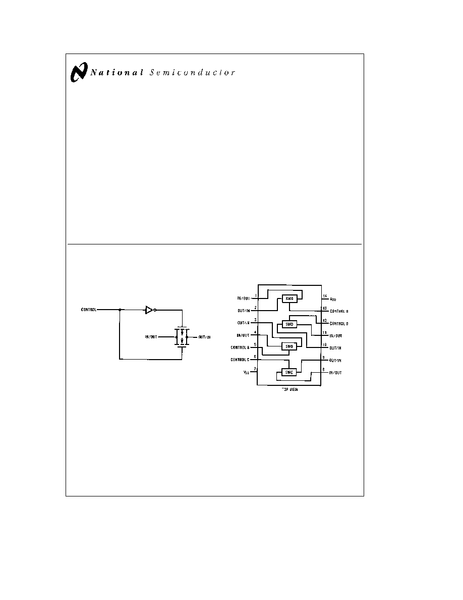
Schematic and Connection Diagrams
Dual-In-Line Package
TLF5661 – 1
Order Number CD4016B
C1995 National Semiconductor Corporation
RRD-B30M105Printed in U S A
相关PDF资料 |
PDF描述 |
|---|---|
| 4016BM | Quad Bilateral Switch |
| 401CMQ045 | SCHOTTKY RECTIFIER |
| 401CMQ | SCHOTTKY RECTIFIER |
| 401CMQ035 | SCHOTTKY RECTIFIER |
| 401CMQ040 | SCHOTTKY RECTIFIER |
相关代理商/技术参数 |
参数描述 |
|---|---|
| 4016BDC | 制造商:Rochester Electronics LLC 功能描述:- Bulk |
| 4016BDM | 制造商:Rochester Electronics LLC 功能描述:- Bulk |
| 4016BDMQB | 制造商:Rochester Electronics LLC 功能描述: 制造商:Texas Instruments 功能描述: |
| 4016BFX | 制造商:Harris Corporation 功能描述: |
| 4016BM | 制造商:NSC 制造商全称:National Semiconductor 功能描述:Quad Bilateral Switch |
发布紧急采购,3分钟左右您将得到回复。