- 您现在的位置:买卖IC网 > PDF目录157231 > 54FCT163TSOB (INTEGRATED DEVICE TECHNOLOGY INC) BINARY COUNTER, PDSO16 PDF资料下载
参数资料
| 型号: | 54FCT163TSOB |
| 厂商: | INTEGRATED DEVICE TECHNOLOGY INC |
| 元件分类: | 计数器 |
| 英文描述: | BINARY COUNTER, PDSO16 |
| 封装: | SOIC-16 |
| 文件页数: | 2/7页 |
| 文件大小: | 115K |
| 代理商: | 54FCT163TSOB |
2
MILITARYANDINDUSTRIALTEMPERATURERANGES
IDT54/74FCT163T/AT/CT
FASTCMOSSYNCHRONOUSPRESETTABLEBINARYCOUNTER
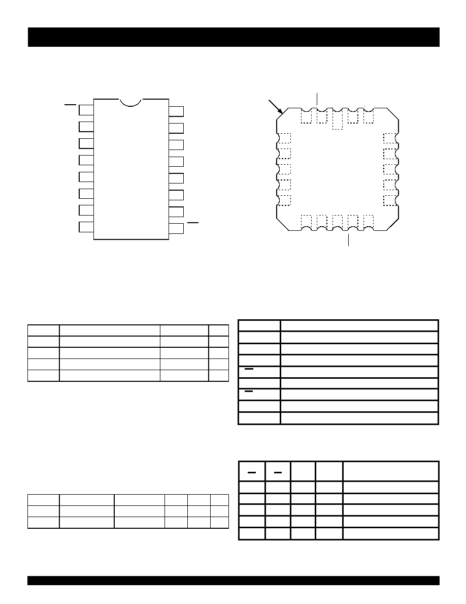
PIN CONFIGURATION
CERDIP/ SOIC/ QSOP/ CERPACK
TOP VIEW
D16-1
SO16-1
SO16-7
E16-1
2
3
4
5
6
7
8
9
10
11
12
13
14
15
16
1
SR
CP
GND
CEP
P0
TC
Q0
Q1
Q2
Q3
CET
PE
VCC
P1
P2
P3
1
2
3
4
5
7
9
6
8
10
11
12
13
14
15
16
17
18
19
20
L20-2
NC
Q0
Q1
Q2
Q3
CP
SR
CEP
GND
NC
PE
CET
NC
V
CC
TC
IN DEX
P0
P1
P3
NC
P2
FUNCTION TABLE(1)
Action on the Rising
SR
PE
CET
CEP
Clock Edge(s)
L
X
Reset (Clear)
H
L
X
Load (Pn
→Qn)
H
Count(Increment)
H
L
X
No Change (Hold)
H
X
L
No Change (Hold)
NOTE:
1. H = HIGH Voltage Level
L = LOW Voltage Level
X = Don’t Care
PIN DESCRIPTION
Pin Names
Description
CEP
Count Enable Parallel Input
CET
Count Enable Trickle Input
C P
Clock Pulse Input (Active Rising Edge)
SR
Synchronous Reset Input (Active LOW)
P0-3
Parallel Data Inputs
PE
Parallel Enable Input (Active LOW)
Q0-3
Flip-FlopOutputs
TC
TerminalCountOutput
LCC
TOP VIEW
ABSOLUTE MAXIMUM RATINGS(1)
Symbol
Rating
Max.
Unit
VTERM(2)
Terminal Voltage with Respect to GND
–0.5 to +7
V
VTERM(3)
Terminal Voltage with Respect to GND
–0.5 to VCC+0.5
V
TSTG
Storage Temperature
–65 to +150
°C
IOUT
DC Output Current
–60 to +120
mA
8T-link
NOTES:
1. Stresses greater than those listed under ABSOLUTE MAXIMUM
RATINGS may cause permanent damage to the device. This is a
stress rating only and functional operation of the device at these or
any other conditions above those indicated in the operational sections
of this specification is not implied. Exposure to absolute maximum
rating conditions for extended periods may affect reliability.
No
terminal voltage may exceed Vcc by +0.5V unless otherwise noted.
2. Inputs and Vcc terminals only.
3. Outputs and I/O terminals only.
CAPACITANCE (TA = +25OC, f = 1.0MHz)
Symbol
Parameter(1)
Conditions
Typ.
Max.
Unit
CIN
Input Capacitance
VIN = 0V
6
10
pF
COUT
Output Capacitance
VOUT = 0V
8
12
pF
8T-link
NOTE:
1. This parameter is measured at characterization but not tested.
相关PDF资料 |
PDF描述 |
|---|---|
| 54FCT245CDB | FCT SERIES, 8-BIT TRANSCEIVER, TRUE OUTPUT, CDIP20 |
| 54FCT374ADB | FCT SERIES, 8-BIT DRIVER, TRUE OUTPUT, CDIP20 |
| 54LS132/BCAJC | LS SERIES, QUAD 2-INPUT NAND GATE, CDIP14 |
| 54LS244/BRAJC | LS SERIES, DUAL 4-BIT DRIVER, TRUE OUTPUT, CDIP20 |
| 54LS26M/B2AJC | LS SERIES, QUAD 2-INPUT NAND GATE, CQCC20 |
相关代理商/技术参数 |
参数描述 |
|---|---|
| 54FCT16823CTEB | 制造商:Integrated Device Technology Inc 功能描述:Flip Flop D-Type Bus Interface Pos-Edge 3-ST 2-Element 56-Pin CFPAK |
| 54FCT191DB | 制造商:IDT 功能描述:54FCT191 IDT |
| 54FCT193ADB | 制造商:IDT 功能描述:54FCT193 IDT |
| 54FCT2245AT | 制造商:IDT 制造商全称:Integrated Device Technology 功能描述:FAST CMOS OCTAL BIDIRECTIONAL TRANSCEIVERS |
| 54FCT2245ATDM | 制造商:未知厂家 制造商全称:未知厂家 功能描述:Single 8-bit Bus Transceiver |
发布紧急采购,3分钟左右您将得到回复。