- 您现在的位置:买卖IC网 > PDF目录117389 > 5962-8768104VEA 1.5 A SWITCHING CONTROLLER, 1000 kHz SWITCHING FREQ-MAX, CDIP16 PDF资料下载
参数资料
| 型号: | 5962-8768104VEA |
| 元件分类: | 稳压器 |
| 英文描述: | 1.5 A SWITCHING CONTROLLER, 1000 kHz SWITCHING FREQ-MAX, CDIP16 |
| 封装: | CERAMIC, DIP-16 |
| 文件页数: | 1/16页 |
| 文件大小: | 267K |
| 代理商: | 5962-8768104VEA |
1
FEATURES
DESCRIPTION
4
5
6
7
3
2
1
8
9
15
10
16
12
14
11
13
CLOCK
RT
CT
RAMP
E/A Out
NI
INV
Error
Amp
Soft Start
ILIM / SD
VCC
GND
VREF
Pwr GND
Out B
Out A
Vc
OSC
PWM Latch
(Set Dom.)
R
S
1.25 V
Wide Bandwidth
Error Amp.
+
Inhibit
ILIM
CPRTR
1 V
1.4 V
9 V
Shutdown
CPRTR
UVLO
VCC Good
Gate
REF
Gen
Internal
Bias
4 V
VREF Good
Output
Inhibit
T
9
A
VIN
Toggler F/F
VDG920322
www.ti.com............................................................................................................................................................................................... SLUS870 – JANUARY 2009
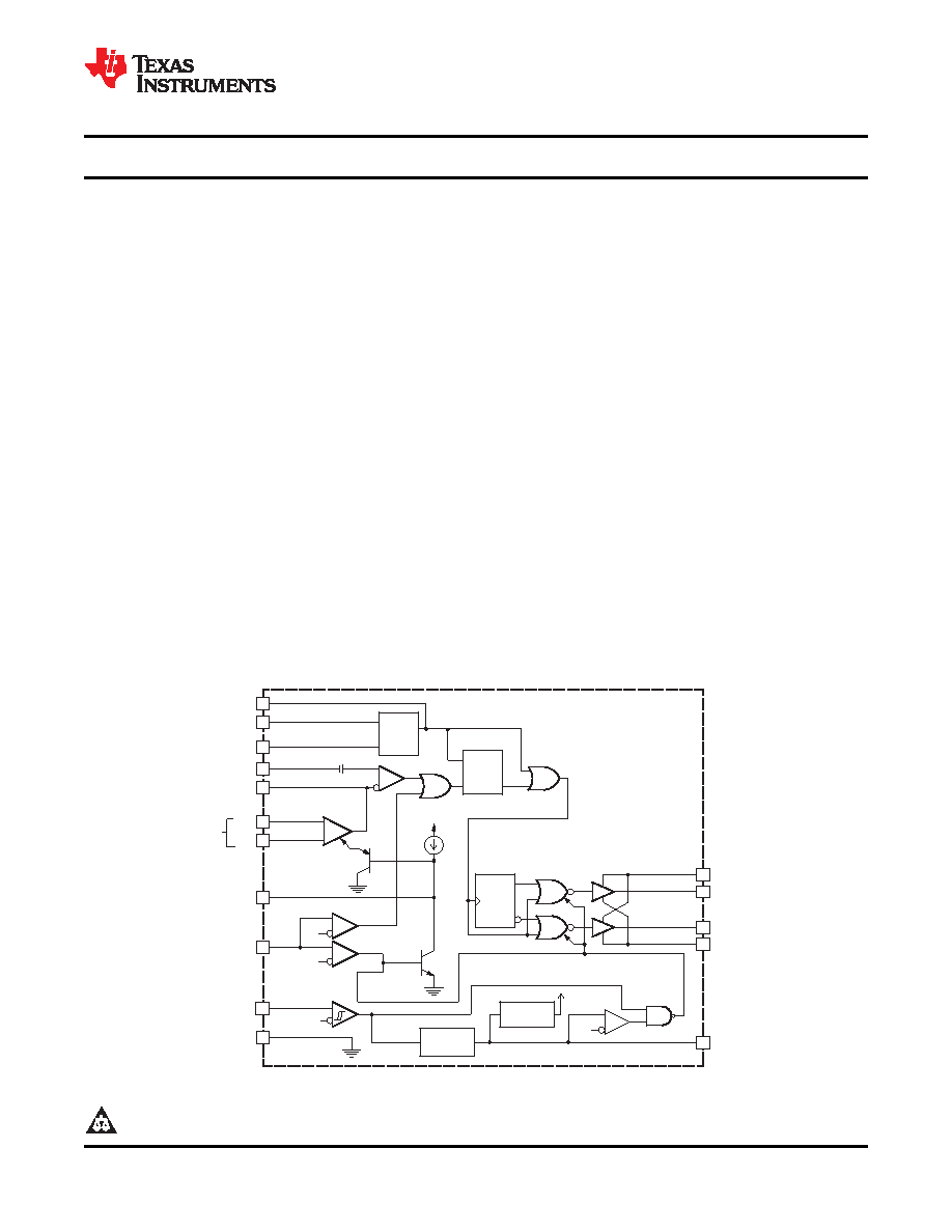
RAD-TOLERANT CLASS V, HIGH-SPEED PWM CONTROLLER
QML-V Qualified, SMD 5962-87681
Rad-Tolerant: 30 kRad (Si) TID (1)
The UC1825 PWM control device is optimized for
high-frequency
switched
mode
power
supply
Compatible With Voltage- or Current-Mode
applications. Particular care was given to minimizing
Topologies
propagation delays through the comparators and
Practical Operation Switching Frequencies to
logic circuitry while maximizing bandwidth and slew
1 MHz
rate of the error amplifier. This controller is designed
for use in either current-mode or voltage mode
50-ns Propagation Delay-to-Output
systems
with
the
capability
for
input
voltage
High-Current Dual Totem Pole Outputs
feed-forward.
(1.5 A Peak)
Protection circuitry includes a current limit comparator
Wide Bandwidth Error Amplifier
with a 1-V threshold, a TTL compatible shutdown
Fully Latched Logic With Double-Pulse
port, and a soft start pin which will double as a
Suppression
maximum duty-cycle clamp. The logic is fully latched
Pulse-by-Pulse Current Limiting
to provide jitter-free operation and prohibit multiple
pulses at an output. An undervoltage lockout section
Soft Start/Maximum Duty-Cycle Control
with 800 mV of hysteresis assures low start up
Undervoltage Lockout With Hysteresis
current. During undervoltage lockout, the outputs are
Low Start-Up Current (1.1 mA)
high impedance.
This device features totem pole outputs designed to
source and sink high peak currents from capacitive
(1)
Radiation tolerance is a typical value based upon initial device
loads, such as the gate of a power MOSFET. The on
qualification with dose rate = 10 mrad/sec. Radiation Lot
Acceptance Testing is available - contact factory for details.
state is designed as a high level.
BLOCK DIAGRAM
1
Please be aware that an important notice concerning availability, standard warranty, and use in critical applications of Texas
Instruments semiconductor products and disclaimers thereto appears at the end of this data sheet.
PRODUCTION DATA information is current as of publication date.
Copyright 2009, Texas Instruments Incorporated
Products conform to specifications per the terms of the Texas
Instruments standard warranty. Production processing does not
necessarily include testing of all parameters.
相关PDF资料 |
PDF描述 |
|---|---|
| 5SC12D | 2-OUTPUT 1.5 W DC-DC UNREG PWR SUPPLY MODULE |
| 5962R1023302QXC | 16-CHANNEL, SGL ENDED MULTIPLEXER, CDFP28 |
| 5IWR1-05-15-N | 2-OUTPUT 1 W DC-DC REG PWR SUPPLY MODULE |
| 5717 | SPECIALTY ANALOG CIRCUIT, XSS3 |
| 5962-0724302HXC | 1-OUTPUT 100 W DC-DC REG PWR SUPPLY MODULE |
相关代理商/技术参数 |
参数描述 |
|---|---|
| 5962-8768105VEA | 制造商:Texas Instruments 功能描述:Current Mode PWM Controller 100mA 16-Pin CDIP 制造商:Texas Instruments 功能描述:UC1825AJ-SP, HIGH SPEED PWM - Rail/Tube |
| 5962-87683012A | 制造商:Texas Instruments 功能描述:Decoder/Demultiplexer Dual 2-to-4 20-Pin LCCC Tube 制造商:Rochester Electronics LLC 功能描述:- Bulk |
| 5962-8768301EA | 制造商:Texas Instruments 功能描述:Decoder/Demultiplexer Dual 2-to-4 16-Pin CDIP Tube 制造商:Rochester Electronics LLC 功能描述:- Bulk |
| 5962-8768301FA | 制造商:Texas Instruments 功能描述:Decoder/Demultiplexer Dual 2-to-4 16-Pin CFPAK Tube 制造商:Rochester Electronics LLC 功能描述:- Bulk |
| 5962-8768401MQA | 制造商:e2v Aerospace & Defense 功能描述:MICROCONTROLLER, 8-BIT, WITH 4K BYTES EPROM MEMORY (3.5 TO 12 MHZ) |
发布紧急采购,3分钟左右您将得到回复。