- 您现在的位置:买卖IC网 > PDF目录68794 > 5962-88565013B QUAD OP-AMP, 600 uV OFFSET-MAX, 6 MHz BAND WIDTH, CQCC28 PDF资料下载
参数资料
| 型号: | 5962-88565013B |
| 元件分类: | 运算放大器 |
| 英文描述: | QUAD OP-AMP, 600 uV OFFSET-MAX, 6 MHz BAND WIDTH, CQCC28 |
| 封装: | CERAMIC, LCC-28 |
| 文件页数: | 4/16页 |
| 文件大小: | 680K |
| 代理商: | 5962-88565013B |
REV. A
OP470
–12–
CAPACITIVE LOAD DRIVING AND POWER
SUPPLY CONSIDERATIONS
The OP470 is unity-gain stable and is capable of driving large
capacitive loads without oscillating. Nonetheless, good supply
bypassing is highly recommended. Proper supply bypassing
reduces problems caused by supply line noise and improves the
capacitive load driving capability of the OP470.
In the standard feedback amplifier, the op amp’s output resistance
combines with the load capacitance to form a low pass filter that
adds phase shift in the feedback network and reduces stability.
A simple circuit to eliminate this effect is shown in Figure 11.
The added components, C1 and R3, decouple the amplifier
from the load capacitance and provide additional stability. The
values of C1 and R3 shown in Figure 11 are for a load capaci-
tance of up to 1000 pF when used with the OP470.
R1
100 *
*
SEE TEXT
R3
50
OP470
C5
0.1 F
*
C4
10 F
+
V–
VOUT
CL
1000pF
C1
1000pF
R2
VIN
PLACE SUPPLY DECOUPLING
CAPACITORS AT OP470
C3
0.1 F
C2
10 F
+
V+
Figure 11. Driving Large Capacitive Loads
In applications where the OP470’s inverting or noninverting
inputs are driven by a low source impedance (under 100
W) or
connected to ground, if V+ is applied before V–, or when V is
disconnected, excessive parasitic currents will flow. Most applica-
tions use dual tracking supplies and with the device supply pins
properly bypassed, power-up will not present a problem. A source
resistance of at least 100
W in series with all inputs (Figure 11)
will limit the parasitic currents to a safe level if V– is discon-
nected. It should be noted that any source resistance, even 100
W,
adds noise to the circuit. Where noise is required to be kept at a
minimum, a germanium or Schottky diode can be used to clamp
the V- pin and eliminate the parasitic current flow instead of
using series limiting resistors. For most applications, only one
diode clamp is required per board or system.
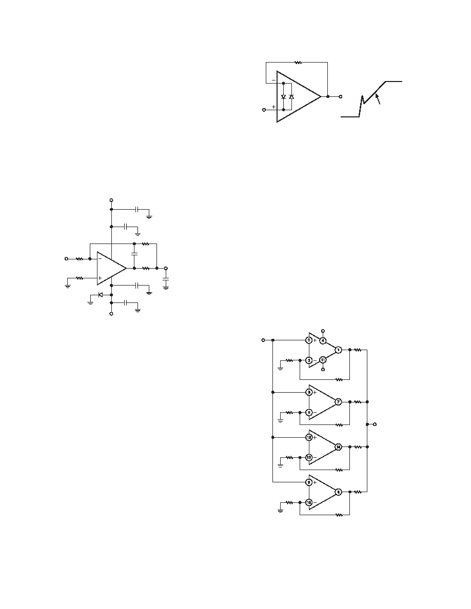
UNITY-GAIN BUFFER APPLICATIONS
When Rf
100 W and the input is driven with a fast, large
signal pulse(> 1 V), the output waveform will look as shown
in Figure 12.
2V/ s
OP470
R1
Figure 12. Pulsed Operation
During the fast feedthrough-like portion of the output, the input
protection diodes effectively short the output to the input, and a
current, limited only by the output short-circuit protection, will
be drawn by the signal generator. With Rf
500 W, the output
is capable of handling the current requirements (IL < 20 mA at
10 V); the amplifier will stay in its active mode and a smooth
transition will occur.
When Rf > 3 k
W, a pole created by Rf and the amplifier’s input
capacitance (2 pF) creates additional phase shift and reduces
phase margin. A small capacitor (20 pF to 50 pF) in parallel
with Rf helps eliminate this problem.
APPLICATIONS
Low Noise Amplifier
A simple method of reducing amplifier noise by paralleling
amplifiers is shown in Figure 13. Amplifier noise, depicted in
Figure 14, is around 2 nV/
÷Hz @ 1 kHz (R.T.I.). Gain for each
paralleled amplifier and the entire circuit is 1000. The 200
W
resistors limit circulating currents and provide an effective out-
put resistance of 50
W. The amplifier is stable with a 10 nF
capacitive load and can supply up to 30 mA of output drive.
R2
50k
1/4
OP470E
+15V
–15V
R3
200
R1
50
VIN
R5
50k
1/4
OP470E
R6
200
R4
50
R8
50k
1/4
OP470E
R9
200
R7
50
R11
50k
1/4
OP470E
R12
200
R10
50
VOUT = 1000VIN
Figure 13. Low Noise Amplifier
相关PDF资料 |
PDF描述 |
|---|---|
| 5962-88565013C | QUAD OP-AMP, 600 uV OFFSET-MAX, 6 MHz BAND WIDTH, CQCC28 |
| 5962-8863001VX | INSTRUMENTATION AMPLIFIER, 80 uV OFFSET-MAX, 0.57 MHz BAND WIDTH, CDIP18 |
| 5962-88630023X | INSTRUMENTATION AMPLIFIER, 150 uV OFFSET-MAX, 0.57 MHz BAND WIDTH, CQCC28 |
| 5962-8863002VX | INSTRUMENTATION AMPLIFIER, 150 uV OFFSET-MAX, 0.57 MHz BAND WIDTH, CDIP18 |
| 5962-88685012A | 1-CHANNEL POWER SUPPLY SUPPORT CKT, CQCC20 |
相关代理商/技术参数 |
参数描述 |
|---|---|
| 5962-8856501CA | 功能描述:仪表放大器 QUAD LOW-NOISE OP AMP IC RoHS:否 制造商:Texas Instruments 通道数量: 输入补偿电压:150 V 可用增益调整: 最大输入电阻:10 kOhms 共模抑制比(最小值):88 dB 工作电源电压:2.7 V to 36 V 电源电流:200 uA 最大工作温度:+ 125 C 最小工作温度:- 40 C 封装 / 箱体:MSOP-8 封装:Bulk |
| 5962-8856501V2A | 制造商:Analog Devices 功能描述:OP AMP, QUAD, LOW-NOISE - Rail/Tube |
| 5962-8856501VCA | 制造商:Analog Devices 功能描述:OP AMP QUAD GP 18V 14CDIP - Rail/Tube |
| 5962-88565022A | 功能描述:高速运算放大器 QUAD HI-SPEED LO-NOISE IC RoHS:否 制造商:Texas Instruments 通道数量:1 电压增益 dB:116 dB 输入补偿电压:0.5 mV 转换速度:55 V/us 工作电源电压:36 V 电源电流:7.5 mA 最大工作温度:+ 85 C 安装风格:SMD/SMT 封装 / 箱体:SOIC-8 封装:Tube 产品: |
| 5962-88565023A | 功能描述:高速运算放大器 QUAD HI-SPEED LO-NOISE IC RoHS:否 制造商:Texas Instruments 通道数量:1 电压增益 dB:116 dB 输入补偿电压:0.5 mV 转换速度:55 V/us 工作电源电压:36 V 电源电流:7.5 mA 最大工作温度:+ 85 C 安装风格:SMD/SMT 封装 / 箱体:SOIC-8 封装:Tube 产品: |
发布紧急采购,3分钟左右您将得到回复。