- 您现在的位置:买卖IC网 > PDF目录68794 > 5962-8863002VX (ANALOG DEVICES INC) INSTRUMENTATION AMPLIFIER, 150 uV OFFSET-MAX, 0.57 MHz BAND WIDTH, CDIP18 PDF资料下载
参数资料
| 型号: | 5962-8863002VX |
| 厂商: | ANALOG DEVICES INC |
| 元件分类: | 测量放大器 |
| 英文描述: | INSTRUMENTATION AMPLIFIER, 150 uV OFFSET-MAX, 0.57 MHz BAND WIDTH, CDIP18 |
| 封装: | CERDIP-18 |
| 文件页数: | 4/22页 |
| 文件大小: | 244K |
| 代理商: | 5962-8863002VX |
AMP01
–12–
REV. D
VOLTAGE GAIN
1M
1
10k
RESISTANCE
–
10k
10
100
1k
VS = 15V
100k
1k
100
RS
RG
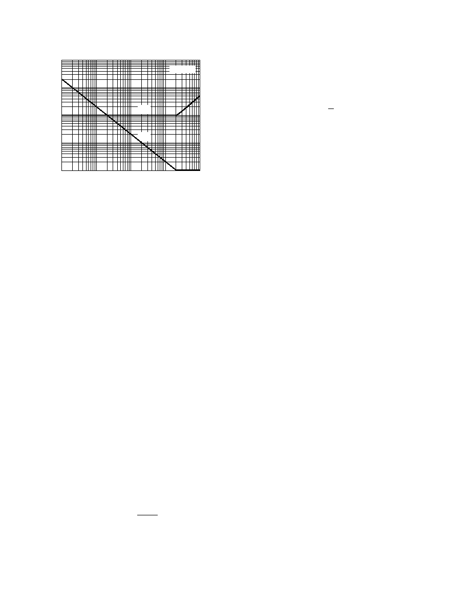
Figure 30. RG and RS Selection
Gain accuracy is determined by the ratio accuracy of RS and RG
combined with the gain equation error of the AMP01 (0.6%
max for A/E grades).
All instrumentation amplifiers require attention to layout so
thermocouple effects are minimized. Thermocouples formed
between copper and dissimilar metals can easily destroy the
TCVOS performance of the AMP01 which is typically
0.15
V/°C. Resistors themselves can generate thermoelectric
EMF’s when mounted parallel to a thermal gradient. “Vishay”
resistors are recommended because a maximum value for ther-
moelectric generation is specified. However, where thermal
gradients are low and gain TCs of 20 ppm–50 ppm are suffi-
cient, general-purpose metal-film resistors can be used for RG
and RS.
COMMON-MODE REJECTION
Ideally, an instrumentation amplifier responds only to the dif-
ference between the two input signals and rejects common-
mode voltages and noise. In practice, there is a small change in
output voltage when both inputs experience the same common-
mode voltage change; the ratio of these voltages is called the
common-mode gain. Common-mode rejection (CMR) is the
logarithm of the ratio of differential-mode gain to common-
mode gain, expressed in dB. CMR specifications are normally
measured with a full-range input voltage change and a specified
source resistance unbalance.
The current-feedback design used in the AMP01 inherently
yields high common-mode rejection. Unlike resistive feedback
designs, typified by the three-op-amp IA, the CMR is not de-
graded by small resistances in series with the reference input. A
slight, but trimmable, output offset voltage change results from
resistance in series with the reference input.
The common-mode input voltage range, CMVR, for linear
operation may be calculated from the formula:
CMVR =
± IVR –
|V OUT|
2 G
(4)
IVR is the data sheet specification for input voltage range; VOUT
is the maximum output signal; G is the chosen voltage gain. For
example, at +25
°C, IVR is specified as ±10.5 volt minimum
with
±15 volt supplies. Using a ±10 volt maximum swing out-
put and substituting the figures in (4) simplifies the formula to:
CMVR =
± 10.5 –
5
G
(5)
For all gains greater than or equal to 10, CMVR is
±10 volt
minimum; at gains below 10, CMVR is reduced.
ACTIVE GUARD DRIVE
Rejection of common-mode noise and line pick-up can be im-
proved by using shielded cable between the signal source and
the IA. Shielding reduces pick-up, but increases input capaci-
tance, which in turn degrades the settling-time for signal
changes. Further, any imbalance in the source resistance be-
tween the inverting and noninverting inputs, when capacitively
loaded, converts the common-mode voltage into a differential
voltage. This effect reduces the benefits of shielding. AC
common-mode rejection is improved by “bootstrapping” the
input cable capacitance to the input signal, a technique called
“guard driving.” This technique effectively reduces the input
capacitance. A single guard-driving signal is adequate at gains
above 100 and should be the average value of the two inputs.
The value of external gain resistor RG is split between two resis-
tors RG1 and RG2; the center tap provides the required signal to
drive the buffer amplifier (Figure 31).
GROUNDING
The majority of instruments and data acquisition systems have
separate grounds for analog and digital signals. Analog ground
may also be divided into two or more grounds which will be tied
together at one point, usually the analog power-supply ground.
In addition, the digital and analog grounds may be joined, nor-
mally at the analog ground pin on the A-to-D converter. Fol-
lowing this basic grounding practice is essential for good circuit
performance (Figure 32).
Mixing grounds causes interactions between digital circuits and
the analog signals. Since the ground returns have finite resis-
tance and inductance, hundreds of millivolts can be developed
between the system ground and the data acquisition compo-
nents. Using separate ground returns minimizes the current flow
in the sensitive analog return path to the system ground point.
Consequently, noisy ground currents from logic gates do not
interact with the analog signals.
Inevitably, two or more circuits will be joined together with their
grounds at differential potentials. In these situations, the differ-
ential input of an instrumentation amplifier, with its high CMR,
can accurately transfer analog information from one circuit to
another.
SENSE AND REFERENCE TERMINALS
The sense terminal completes the feedback path for the instru-
mentation amplifier output stage and is normally connected
directly to the output. The output signal is specified with re-
spect to the reference terminal, which is normally connected to
analog ground.
相关PDF资料 |
PDF描述 |
|---|---|
| 5962-88685012A | 1-CHANNEL POWER SUPPLY SUPPORT CKT, CQCC20 |
| TL7705AMFKB | 1-CHANNEL POWER SUPPLY SUPPORT CKT, CQCC20 |
| 5962-88685042A | 1-CHANNEL POWER SUPPLY SUPPORT CKT, CQCC20 |
| 5962-8868505PA | 1-CHANNEL POWER SUPPLY SUPPORT CKT, CDIP8 |
| 5962-8868505HA | 1-CHANNEL POWER SUPPLY SUPPORT CKT, CDFP10 |
相关代理商/技术参数 |
参数描述 |
|---|---|
| 5962-8863003V3A | 制造商:Analog Devices 功能描述:AEROSPACE LOW-NOISE PRECISION INSTRUMENTATION AMPLIFIER - Rail/Tube |
| 5962-8863003VKA | 制造商:Analog Devices 功能描述:MICROCIRCUIT, LINEAR, INSTRUMENTATION AMPLIFIER - Rail/Tube |
| 5962-8863003VVA | 制造商:Analog Devices 功能描述:MICROCIRCUIT, LINEAR, INSTRUMENTATION AMPLIFIER, MONOLITHIC - Rail/Tube |
| 59628863101PA | 制造商: 功能描述: 制造商:National Semiconductor Corporation 功能描述: 制造商:undefined 功能描述: |
| 5962-8863401UC | 制造商:Intersil Corporation 功能描述:EEPROM PARALLEL 256KBIT 32KX8 5V - Rail/Tube |
发布紧急采购,3分钟左右您将得到回复。