- 您现在的位置:买卖IC网 > PDF目录67329 > 5962-8992002VA (TEXAS INSTRUMENTS INC) 1 A SWITCHING CONTROLLER, 500 kHz SWITCHING FREQ-MAX, CDIP18 PDF资料下载
参数资料
| 型号: | 5962-8992002VA |
| 厂商: | TEXAS INSTRUMENTS INC |
| 元件分类: | 稳压器 |
| 英文描述: | 1 A SWITCHING CONTROLLER, 500 kHz SWITCHING FREQ-MAX, CDIP18 |
| 封装: | CERAMIC, DIP-18 |
| 文件页数: | 7/14页 |
| 文件大小: | 1121K |
| 代理商: | 5962-8992002VA |
PARAMETER
TEST CONDITIONS
UC1841 / UC2841
UC3841
UNITS
MIN
TYP
MAX
MIN
TYP
MAX
Power Inputs
Start-Up Current
VIN = 30V, Pin 2 = 2.5V
4.5
6
4.5
6
mA
Operating Current
VIN = 30V, Pin 2 = 3.5V
10
14
10
14
mA
Supply OV Clamp
IIN = 20mA
33
40
45
33
40
45
V
Reference Section
Reference Voltage
TJ = 25°C
4.95
5.0
5.05
4.9
5.0
5.1
V
Line Regulation
VIN = 8 to 30V
10
15
10
20
mV
Load Regulation
IL = 0 to 10mA
1020
1030
mV
Temperature Stability
Over Operating Temperature Range
4.9
5.1
4.85
5.15
V
Short Circuit Current
VREF = 0, TJ = 25°C
-80
-100
-80
-100
mA
Oscillator
Nominal Frequency
TJ = 25°C
47
50
53
45
50
55
kHz
Voltage Stability
VIN = 8 to 30V
0.5
1
0.5
1
%
Temperature Stability
Over Operating Temperature Range
45
55
43
57
kHz
Maximum Frequency
RT = 2k
, CT = 330pF
500
kHz
UC1841
UC2841
UC3841
ELECTRICAL CHARACTERISTICS: Unless otherwise stated, these specifications apply for TA = -55°C to +125°C for the
UC1841, -25°C to +85°C for the UC2841, and 0°C to +70°C for the UC3841; VIN = 20V, RT = 20k
, CT = .001mfd, RR = 10k,
CR = .001mfd, Current Limit Threshold = 200mV, TA = TJ.
Supply Voltage, +VIN (Pin 15) (Note 2)
Voltage Driven . . . . . . . . . . . . . . . . . . . . . . . . . . . . . . . . . +32V
Current Driven, 100mA maximum . . . . . . . . . . . . Self-limiting
PWM Output Voltage (Pin 12) . . . . . . . . . . . . . . . . . . . . . . . 40V
PWM Output Current, Steady-State (Pin 12) . . . . . . . . . 400mA
PWM Output Peak Energy Discharge . . . . . . . . . . . . 20
Joules
Driver Bias Current (Pin 14) . . . . . . . . . . . . . . . . . . . . . -200mA
Reference Output Current (Pin 16) . . . . . . . . . . . . . . . . -50mA
Slow-Start Sink Current (Pin 8) . . . . . . . . . . . . . . . . . . . . 20mA
VIN Sense Current (Pin 11). . . . . . . . . . . . . . . . . . . . . . . . 10mA
Current Limit Inputs (Pins 6 & 7) . . . . . . . . . . . . . -0.5 to +5.5V
Stop Input (Pin 4) . . . . . . . . . . . . . . . . . . . . . . . . . -0.3 to +5.5V
Comparator Inputs
(Pins 1, 7, 9-11, 16) . . . . . . . . . . . . Internally clamped at 12V
Power Dissipation at TA = 25°C (Note 3) . . . . . . . . . . . 1000mW
Power Dissipation at TC = 25°C (Note 3) . . . . . . . . . . . 2000mW
Operating Junction Temperature . . . . . . . . . . -55°C to +150°C
Storage Temperature Range. . . . . . . . . . . . . . -65°C to +150°C
Lead Temperature (Soldering, 10 sec) . . . . . . . . . . . . . +300°C
Note 1: All voltages are with respect to ground, Pin 13.
Currents are positive-into, negative-out of the specified
terminal.
Note 2: All pin numbers are referenced to DIL-18 package.
Note 3: Consult Packaging Section of Databook for thermal
limitations and considerations of package.
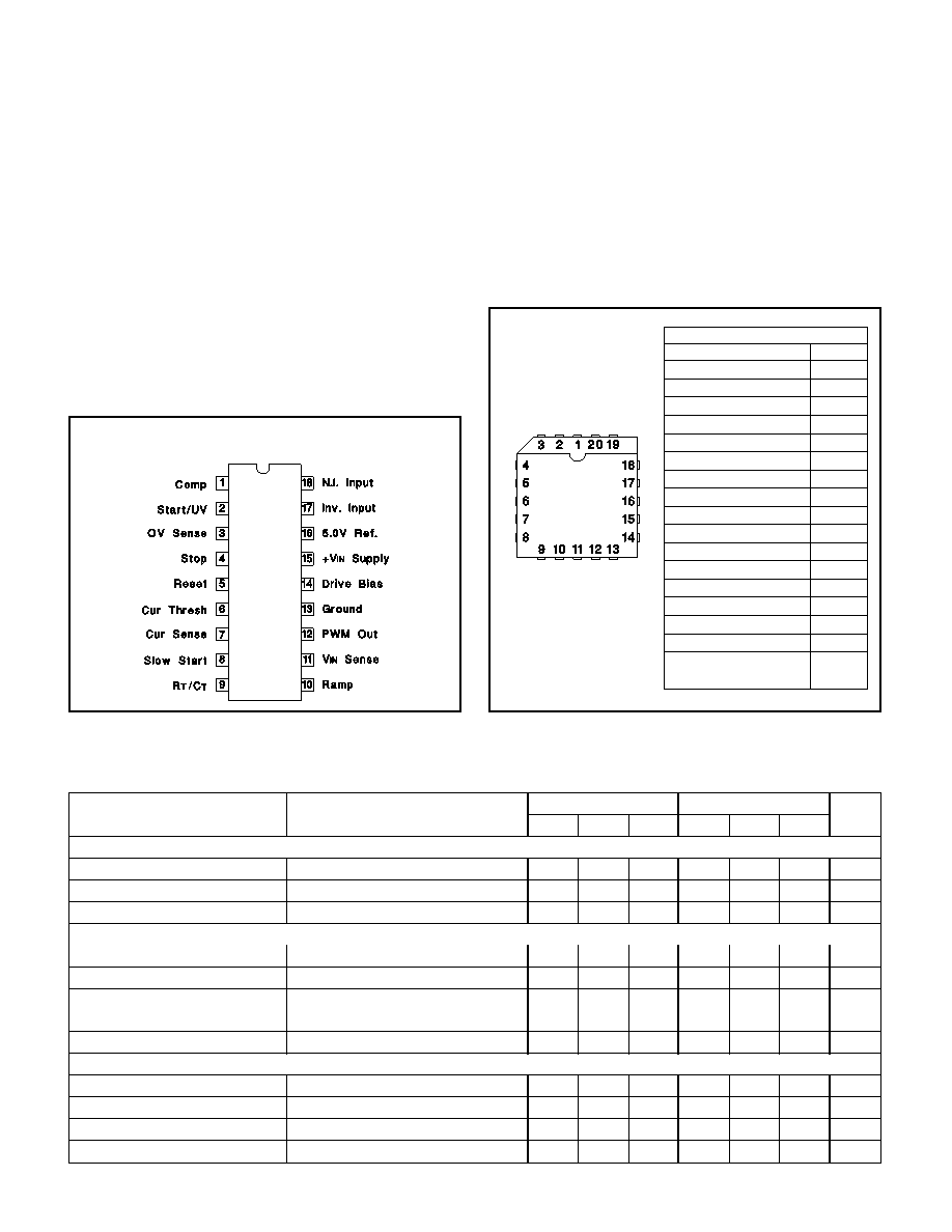
CONNECTION DIAGRAMS
PLCC-20, LCC-20
(TOP VIEW)
Q or L Package
DIL-18, SOIC-18 (TOP VIEW)
J or N, DW Package
PACKAGE PIN FUNCTIONS
FUNCTION
PIN
Comp
1
Start/UV
2
OV Sense
3
Stop
4
Reset
5
CUR Thresh
7
CUR Sense
8
Slow Start
9
RT/CT
10
Ramp
11
VIN Sense
12
PWM Out
13
Ground
14
Drive Bias
15
+VIN Supply
17
5.0V REF
18
Inv. Input
19
N.I. Input
20
ABSOLUTE MAXIMUM RATINGS
2
相关PDF资料 |
PDF描述 |
|---|---|
| 5962-8992101XX | 1-OUTPUT TWO TERM VOLTAGE REFERENCE, 6.9 V, MBCY2 |
| LM129AH883B | 1-OUTPUT THREE TERM VOLTAGE REFERENCE, MBCY3 |
| 5962-89932012A | PARALLEL, 8 BITS INPUT LOADING, 0.085 us SETTLING TIME, 8-BIT DAC, CQCC20 |
| 5962-8995701VA | BRUSH DC MOTOR CONTROLLER, 0.5 A, CDIP18 |
| 5962-89957012A | BRUSH DC MOTOR CONTROLLER, 0.5 A, CQCC20 |
相关代理商/技术参数 |
参数描述 |
|---|---|
| 59628992501EA | 制造商:TI 功能描述:SNJ54LS378J |
| 5962-8992501EA | 制造商:Texas Instruments 功能描述:Flip Flop D-Type Bus Interface Pos-Edge 1-Element 16-Pin CDIP Tube 制造商:Rochester Electronics LLC 功能描述:- Bulk 制造商:Texas Instruments 功能描述:FLIP FLOP D-TYPE BUS INTRFC POS-EDGE 1-ELEM 16CDIP - Rail/Tube |
| 5962-8992801XA | 制造商:Rochester Electronics LLC 功能描述:- Bulk |
| 5962-8992901VXA | 制造商:Analog Devices 功能描述:V-Ref Precision 1.235V 5mA 2-Pin TO-51 Tube 制造商:Analog Devices 功能描述:V-REF PRECISION 1.235V 5MA 2PIN TO-51 - Rail/Tube |
| 5962-8993001MIA | 制造商:e2v 功能描述: 制造商:e2v technologies 功能描述: |
发布紧急采购,3分钟左右您将得到回复。