- 您现在的位置:买卖IC网 > PDF目录63397 > 5962-9083801HX (MS KENNEDY CORP) DUAL OP-AMP, 1500 uV OFFSET-MAX, MBFM8 PDF资料下载
参数资料
| 型号: | 5962-9083801HX |
| 厂商: | MS KENNEDY CORP |
| 元件分类: | 运算放大器 |
| 英文描述: | DUAL OP-AMP, 1500 uV OFFSET-MAX, MBFM8 |
| 封装: | HERMETIC SEALED, TO-3, 8 PIN |
| 文件页数: | 2/6页 |
| 文件大小: | 290K |
| 代理商: | 5962-9083801HX |
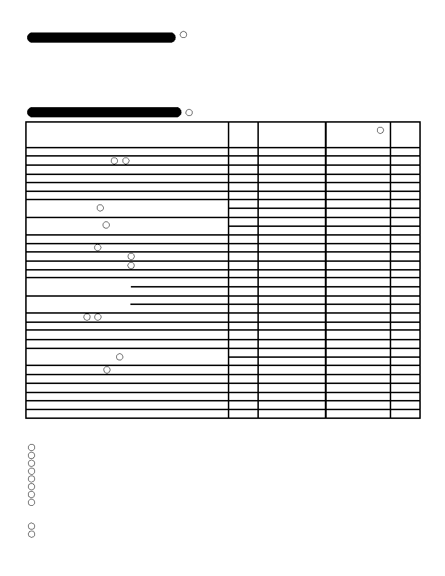
Group A
Subgroup
-
1, 2, 3
1
2, 3
1
2, 3
1
2, 3
-
4
5, 6
4
5, 6
-
4
5, 6
-
Parameter
STATIC
Supply Voltage Range
Quiescent Current
INPUT
Input Offset Voltage
Input Offset Voltage Drift
Input Capacitance
Input Impedance
Common Mode Rejection Ratio
Power Supply Rejection Ratio
OUTPUT
Settling Time
Power Bandwidth
TRANSFER CHARACTERISTICS
Slew Rate
THERMAL RESISTANCE
θJC (Junction to Case)
θJC
θJA (Junction to Ambient)
Test Conditions
Total - Both Amplifiers VIN = 0V
VIN = 0V
VCM = 0V
Either Input
F = DC
F = DC VCM = ±22V
VCC = ±10V to ±40V
RL = 5.6 F ≤ 10 KHz
RL = 10 F = 10 KHz
RL = 5.6 F ≤ 10 KHz
RL = 10 F = 10 KHz
0.1% 2V step
RL = 10 VO = 20 VRMS
VOUT = ±10V RL = 10
One Amplifier, DC Output
One Amplifier, AC Output F > 60 Hz
Both Amplifiers, DC Output
Both Amplifiers, AC Output F > 60 Hz
No Heat Sink
Max.
±40
±60
±10
-
±100
-
30
-
2.2
1.8
1.5
1.3
-
Typ.
±35
±40
±1.0
±15
±4
±10
2.0
-
5
1012
113
90
±29
-
±8
-
2
50
10
100
-
1.9
1.7
1.2
1.1
30
Min.
±10
-
90
-
±28
-
±5
-
40
6
90
-
Typ.
±35
±40
±0.1
±15
±4
±10
2.0
-
5
1012
113
90
±29
±31
±8
-
2
55
10
100
-
1.4
1.25
0.9
0.8
30
Min.
±10
-
95
-
±28
±30
±5
±3.0
-
45
6
95
85
-
±VCC Voltage Supply
±40V
IOUT
Peak Output Current
See S.O.A.
VIN
Differential Input Voltage
±VCC
VIN
Common Mode Input Voltage
±VCC
TC
Case Operating Temperature Range
MSK 2541B/E
-55° to +125°C
MSK 2541
-40° to +85°C
ABSOLUTE MAXIMUM RATINGS
TST
Storage Temperature Range
-65° to +150°C
TLD
Lead Temperature Range
300°C
(10 Seconds)
TJ
Junction Temperature
150°C
Units
V
mA
mV
V/°C
pA
nA
pA
nA
pF
W
dB
V
A
S
KHz
V/S
dB
°C/W
2
Rev. H 2/08
ELECTRICAL SPECIFICATIONS
4
3 4
Max.
±40
±60
±1.5
±50
±150
30
50
-
1.9
1.5
1.2
1.0
-
Unless otherwise specified: ±VCC = ±34 VDC, all specs are per amplifier.
Electrical specifications are derated for power supply voltages other than ±34 VDC.
AV = -1, measured in false summing junction circuit.
Devices shall be capable of meeting the parameter, but need not be tested. Typical parameters are for reference only.
Industrial and E grade devices shall be tested to subgroups 1 and 4 unless otherwise specified.
Military grade devices ('B' suffix) shall be 100% tested to subgroups 1, 2, 3 and 4.
Subgroup 5 and 6 testing available upon request.
Subgroup 1, 4
TA=TC=+25°C
Subgroup 2, 5
TA=TC=+125°C
Subgroup 3, 6
TA=TC=-55°C
Reference DSCC SMD 5962-9083801 and 5962-9083803 for electrical specifications for devices purchased as such.
Continuous operation at or above absolute maximum ratings may adversely effect the device performance and/or life cycle.
4
2
4
Input Bias Current
Input Offset Current
VCM = 0V
Output Current
Output Voltage Swing
Open Loop Voltage Gain
F = 10 Hz RL = 10 K
MSK 2541B/E
MSK 2541
4
5
○○
○○○○○○○○○
○
○○○○○
○○○○○○○○
○
○○○○○
○○○○○○○○
○
○○○○○○○○○○○
○
○○○○○○
○
○○○○○○
○○○○○
4
9
1
2
3
4
5
6
7
8
9
10
NOTES:
10
相关PDF资料 |
PDF描述 |
|---|---|
| 5962-9083803HX | DUAL OP-AMP, 1500 uV OFFSET-MAX, MBFM8 |
| 5962-9089401MEX | INSTRUMENTATION AMPLIFIER, 500 uV OFFSET-MAX, 4 MHz BAND WIDTH, CDIP16 |
| 5962-9091101MXX | PARALLEL, WORD INPUT LOADING, 0.022 us SETTLING TIME, 12-BIT DAC, CDIP28 |
| 5962-9091401MXX | 1-OUTPUT TWO TERM VOLTAGE REFERENCE, 1.24 V, MBCY3 |
| 5962-9098701Q2A | PLL FREQUENCY SYNTHESIZER, 10 MHz |
相关代理商/技术参数 |
参数描述 |
|---|---|
| 5962-9083801HXA | 制造商:International Rectifier 功能描述:POWER OPERATIONAL AMPLIFIER |
| 5962-9083801HXA-R | 制造商:International Rectifier 功能描述: |
| 5962-9084101MCA | 制造商:Linear Technology 功能描述:POWER SUPPLY-VOLTAGE REGULATOR |
| 5962-9084501MPA | 制造商:Rochester Electronics LLC 功能描述:- Bulk |
| 5962-9084701MRA | 制造商:Micross Components, Inc. 功能描述:DRAM, 4MB - Rail/Tube |
发布紧急采购,3分钟左右您将得到回复。