- 您现在的位置:买卖IC网 > PDF目录67334 > 5962-9167302QXA (NATIONAL SEMICONDUCTOR CORP) 3.2 A SWITCHING REGULATOR, 62 kHz SWITCHING FREQ-MAX, MBFM2 PDF资料下载
参数资料
| 型号: | 5962-9167302QXA |
| 厂商: | NATIONAL SEMICONDUCTOR CORP |
| 元件分类: | 稳压器 |
| 英文描述: | 3.2 A SWITCHING REGULATOR, 62 kHz SWITCHING FREQ-MAX, MBFM2 |
| 封装: | TO-3, 4 PIN |
| 文件页数: | 27/29页 |
| 文件大小: | 658K |
| 代理商: | 5962-9167302QXA |
第1页第2页第3页第4页第5页第6页第7页第8页第9页第10页第11页第12页第13页第14页第15页第16页第17页第18页第19页第20页第21页第22页第23页第24页第25页第26页当前第27页第28页第29页
All Output Voltage Versions
Electrical Characteristics (Continued)
Specifications with standard type face are for T
J = 25C, and those with boldface type apply over full Operating Temperature
Range. Unless otherwise specified, V
IN = 12V for the 3.3V, 5V, and Adjustable version, VIN = 25V for the 12V version, and VIN
= 30V for the 15V version. I
LOAD = 200 mA.
Symbol
Parameter
Conditions
Typ
LM1575-XX
LM2575-XX
Units
(Limits)
LM2575HV-XX
Limit
(Note 2)
(Note 3)
ON /OFF CONTROL Test Circuit
Figure 2
V
IH
ON /OFF Pin Logic
V
OUT = 0V
1.4
2.2/2.4
V(Min)
V
IL
Input Level
V
OUT = Nominal Output Voltage
1.2
1.0/0.8
V(Max)
I
IH
ON /OFF Pin Input
ON /OFF Pin = 5V (OFF)
12
A
Current
30
A(Max)
I
IL
ON /OFF Pin = 0V (ON)
0A
10
A(Max)
Note 1: Absolute Maximum Ratings indicate limits beyond which damage to the device may occur. Operating Ratings indicate conditions for which the device is in-
tended to be functional, but do not guarantee specific performance limits. For guaranteed specifications and test conditions, see the Electrical Characteristics.
Note 2: All limits guaranteed at room temperature (standard type face) and at temperature extremes (bold type face). All limts are used to calculate Average Out-
going Quality Level, and all are 100% production tested.
Note 3: All limits guaranteed at room temperature (standard type face) and at temperature extremes (bold type face). All room temperature limits are 100% pro-
duction tested. All limits at temperature extremes are guaranteed via correlation using standard Statistical Quality Control (SQC) methods.
Note 4: External components such as the catch diode, inductor, input and output capacitors can affect switching regulator system performance. When the LM1575/
LM2575 is used as shown in the
Figure 2 test circuit, system performance will be as shown in system parameters section of Electrical Characteristics.
Note 5: Output (pin 2) sourcing current. No diode, inductor or capacitor connected to output pin.
Note 6: Feedback (pin 4) removed from output and connected to 0V.
Note 7: Feedback (pin 4) removed from output and connected to +12V for the Adjustable, 3.3V, and 5V versions, and +25V for the 12V and 15V versions, to force
the output transistor OFF.
Note 8: VIN = 40V (60V for the high voltage version).
Note 9: Junction to ambient thermal resistance (no external heat sink) for the 5 lead TO-220 package mounted vertically, with 12 inch leads in a socket, or on a PC
board with minimum copper area.
Note 10: Junction to ambient thermal resistance (no external heat sink) for the 5 lead TO-220 package mounted vertically, with 12 inch leads soldered to a PC board
containing approximately 4 square inches of copper area surrounding the leads.
Note 11: Junction to ambient thermal resistance with approxmiately 1 square inch of pc board copper surrounding the leads. Additional copper area will lower thermal
resistance further. See thermal model in Switchers made Simple software.
Note 12: If the TO-263 package is used, the thermal resistance can be reduced by increasing the PC board copper area thermally connected to the package: Using
0.5 square inches of copper area,
θJA is 50C/W; with 1 square inch of copper area, θJA is 37C/W; and with 1.6 or more square inches of copper area, θJA is 32C/W.
Note 13: The oscillator frequency reduces to approximately 18 kHz in the event of an output short or an overload which causes the regulated output voltage to drop
approximately 40% from the nominal output voltage. This self protection feature lowers the average power dissipation of the IC by lowering the minimum duty cycle
from 5% down to approximately 2%.
Note 14: Refer to RETS LM1575J for current revision of military RETS/SMD.
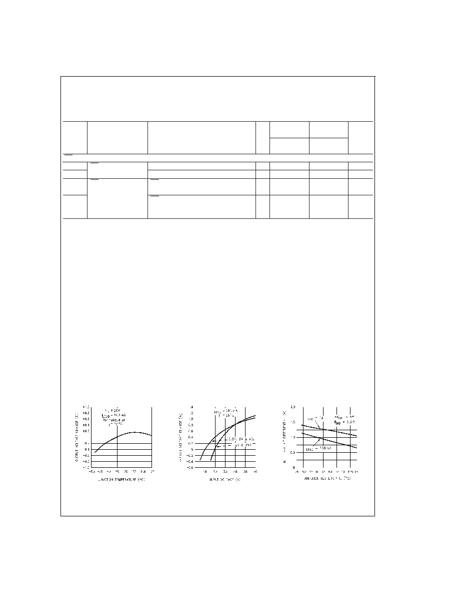
Typical Performance Characteristics (Circuit of Figure 2)
Normalized Output Voltage
DS011475-32
Line Regulation
DS011475-33
Dropout Voltage
DS011475-34
www.national.com
7
相关PDF资料 |
PDF描述 |
|---|---|
| 5962-9167202QXA | 3.2 A SWITCHING REGULATOR, 62 kHz SWITCHING FREQ-MAX, MBFM2 |
| 5962-9167102QXA | 3.2 A SWITCHING REGULATOR, 62 kHz SWITCHING FREQ-MAX, MBFM2 |
| 5962-9167401QEA | 3 A SWITCHING REGULATOR, 58 kHz SWITCHING FREQ-MAX, CDIP16 |
| 5962-9167401QXA | 3 A SWITCHING REGULATOR, 58 kHz SWITCHING FREQ-MAX, MBFM2 |
| 5962-9167401QZA | 3 A SWITCHING REGULATOR, 58 kHz SWITCHING FREQ-MAX, CDSO16 |
相关代理商/技术参数 |
参数描述 |
|---|---|
| 5962-9167601HXA | 制造商:Micropac Industries Inc 功能描述:Optocoupler Logic-Out Open Collector DC-IN 1-CH 6-Pin 制造商:Micropac Industries, Inc. 功能描述:Optocoupler Logic-Out Open Collector DC-IN 1-CH 6-Pin |
| 59629167702MZA | 制造商:Integrated Device Technology Inc 功能描述:FIFO Mem Async Dual Depth/Width Uni-Dir 8K x 9 32-Pin LLCC |
| 5962-9167703MXA | 制造商:Integrated Device Technology Inc 功能描述:FIFO ASYNC DUAL DEPTH/WIDTH UNI-DIR 8KX9 28CDIP - Rail/Tube |
| 5962-9167703MYA | 制造商:Integrated Device Technology Inc 功能描述:FIFO ASYNC DUAL DEPTH/WIDTH UNI-DIR 8KX9 28CDIP - Rail/Tube |
| 5962-9167703MZA | 功能描述:先进先出 RoHS:否 制造商:IDT 电路数量: 数据总线宽度:18 bit 总线定向:Unidirectional 存储容量:4 Mbit 定时类型:Synchronous 组织:256 K x 18 最大时钟频率:100 MHz 访问时间:10 ns 电源电压-最大:3.6 V 电源电压-最小:6 V 最大工作电流:35 mA 最大工作温度:+ 85 C 封装 / 箱体:TQFP-80 封装: |
发布紧急采购,3分钟左右您将得到回复。