- 您现在的位置:买卖IC网 > PDF目录68797 > 5962-9452101M2A (ANALOG DEVICES INC) QUAD OP-AMP, 75 uV OFFSET-MAX, CQCC20 PDF资料下载
参数资料
| 型号: | 5962-9452101M2A |
| 厂商: | ANALOG DEVICES INC |
| 元件分类: | 运算放大器 |
| 英文描述: | QUAD OP-AMP, 75 uV OFFSET-MAX, CQCC20 |
| 封装: | CERAMIC, LCC-20 |
| 文件页数: | 10/12页 |
| 文件大小: | 297K |
| 代理商: | 5962-9452101M2A |
REV. D
OP497
–7–
APPLICATIONS INFORMATION
Extremely low bias current over the full military temperature range
makes the OP497 attractive for use in sample-and-hold amplifiers,
peak detectors, and log amplifiers that must operate over a wide
temperature range. Balancing input resistances is not necessary
with the OP497. Offset voltage and TCVOS are degraded only
minimally by high source resistance, even when unbalanced.
The input pins of the OP497 are protected against large differen-
tial voltage by back-to-back diodes and current-limiting resistors.
Common-mode voltages at the inputs are not restricted, and may
vary over the full range of the supply voltages used.
The OP497 requires very little operating headroom about the
supply rails, and is specified for operation with supplies as low
as
± 2 V. Typically, the common-mode range extends to within
1 V of either rail. The output typically swings to within 1 V of
the rails when using a 10 k
load.
AC PERFORMANCE
The OP497’s ac characteristics are highly stable over its full
operating temperature range. Unity-gain small-signal response is
shown in Figure 1. Extremely tolerant of capacitive loading on
the output, the OP497 displays excellent response even with
1000 pF loads (Figure 2).
10
90
100
0%
20mV
5 s
Figure 1. Small-Signal Transient Response
(CLOAD = 100 pF, AVCL = 1)
10
90
100
0%
20MV
5 s
Figure 2. Small-Signal Transient Response
(CLOAD = 1000 pF, AVCL = 1)
10
90
100
0%
2V
50 s
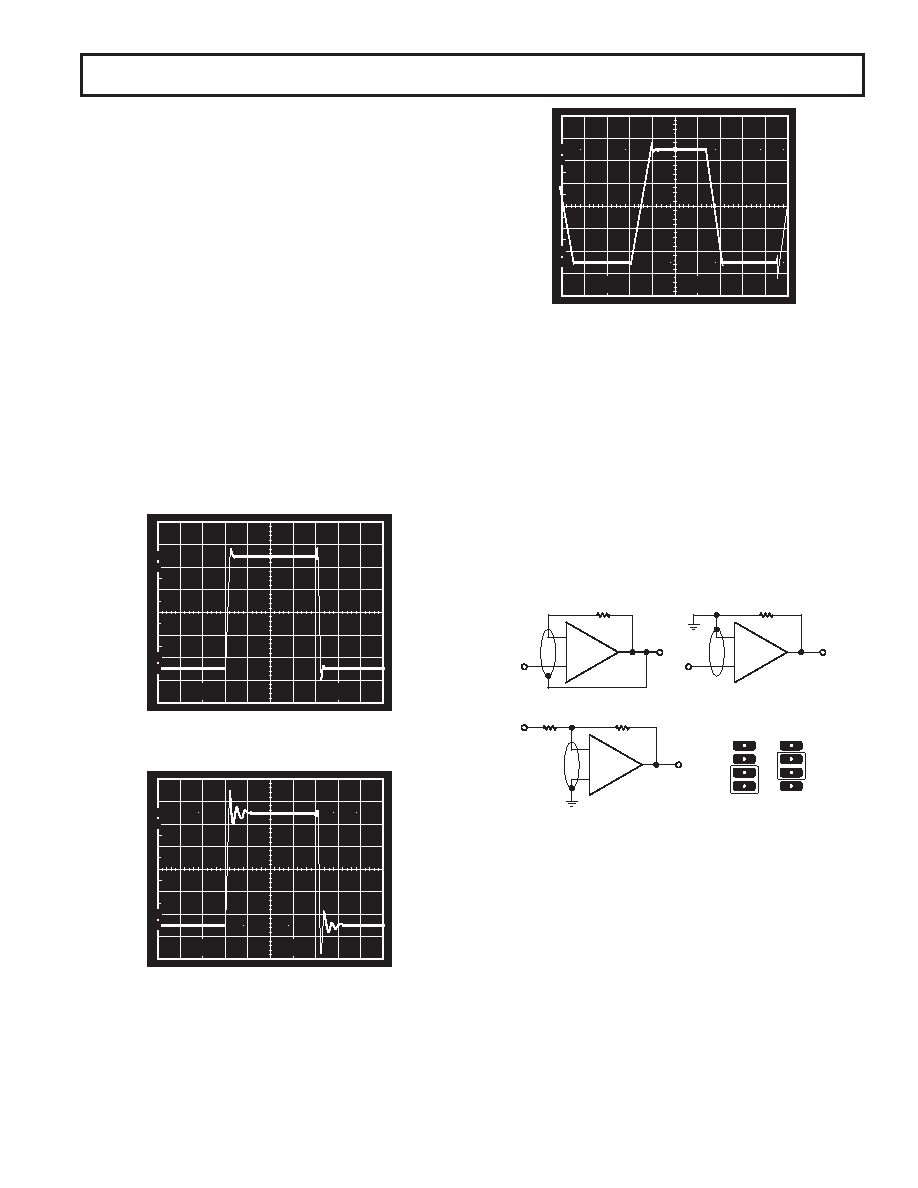
Figure 3. Large-Signal Transient Response (AVCL = 1)
GUARDING AND SHIELDING
To maintain the extremely high input impedances of the OP497,
care must be taken in circuit board layout and manufacturing.
Board surfaces must be kept scrupulously clean and free of mois-
ture. Conformal coating is recommended to provide a humidity
barrier. Even a clean PC board can have 100 pA of leakage currents
between adjacent traces, so guard rings should be used around
the inputs. Guard traces are operated at a voltage close to that
on the inputs, as shown in Figure 4, so that leakage currents
become minimal. In noninverting applications, the guard ring
should be connected to the common-mode voltage at the invert-
ing input. In inverting applications, both inputs remain at ground,
so the guard trace should be grounded. Guard traces should be
on both sides of the circuit board.
1/4
OP497
UNITY GAIN FOLLOWER
NONINVERTING AMPLIFIER
INVERTING AMPLIFIER
B
8
A
1
MINI-DIP
BOTTOM VIEW
–
+
–
+
–
+
1/4
OP497
1/4
OP497
Figure 4. Guard Ring Layout and Connections
相关PDF资料 |
PDF描述 |
|---|---|
| 5962-9452101MCA | QUAD OP-AMP, 75 uV OFFSET-MAX, CDIP14 |
| 5962-9455301M2X | QUAD OP-AMP, 350 uV OFFSET-MAX, 4 MHz BAND WIDTH, CQCC20 |
| 5962-9455301MCX | QUAD OP-AMP, 350 uV OFFSET-MAX, 4 MHz BAND WIDTH, CDIP14 |
| 5962-9460202Q2A | DUAL OP-AMP, 10500 uV OFFSET-MAX, 9.4 MHz BAND WIDTH, CQCC20 |
| 5962-9460202QPA | DUAL OP-AMP, 10500 uV OFFSET-MAX, 9.4 MHz BAND WIDTH, CDIP8 |
相关代理商/技术参数 |
参数描述 |
|---|---|
| 5962-9452201MXA | 制造商:Cypress Semiconductor 功能描述: |
| 5962-9452201MXX | 制造商:Cypress Semiconductor 功能描述: 制造商:Rochester Electronics LLC 功能描述: |
| 5962-9452601Q2A | 制造商:Texas Instruments 功能描述:Comparator Dual |
| 5962-9452601QPA | 制造商:Texas Instruments 功能描述:Comparator Dual 制造商:Texas Instruments 功能描述:COMPARATOR DUAL 18V/36V 8CDIP - Rail/Tube |
| 59629452602MGA | 制造商:Texas Instruments 功能描述:_ |
发布紧急采购,3分钟左右您将得到回复。