- 您现在的位置:买卖IC网 > PDF目录157280 > 5962-9855202QXX 32-BIT, 16 MHz, RISC MICROCONTROLLER, CPGA144 PDF资料下载
参数资料
| 型号: | 5962-9855202QXX |
| 元件分类: | 微控制器/微处理器 |
| 英文描述: | 32-BIT, 16 MHz, RISC MICROCONTROLLER, CPGA144 |
| 封装: | CERAMIC, PGA-144 |
| 文件页数: | 9/64页 |
| 文件大小: | 1464K |
| 代理商: | 5962-9855202QXX |
第1页第2页第3页第4页第5页第6页第7页第8页当前第9页第10页第11页第12页第13页第14页第15页第16页第17页第18页第19页第20页第21页第22页第23页第24页第25页第26页第27页第28页第29页第30页第31页第32页第33页第34页第35页第36页第37页第38页第39页第40页第41页第42页第43页第44页第45页第46页第47页第48页第49页第50页第51页第52页第53页第54页第55页第56页第57页第58页第59页第60页第61页第62页第63页第64页
17
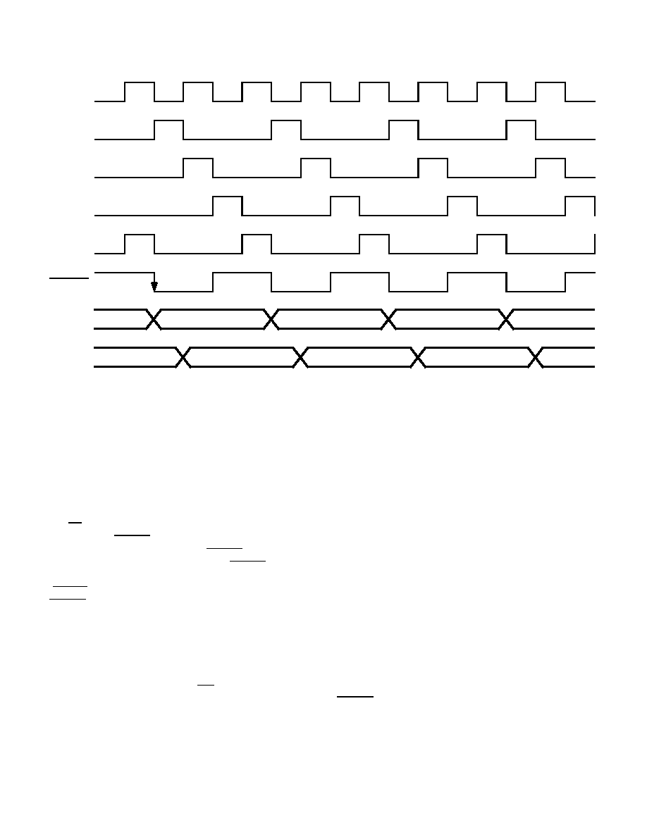
If the instruction being executed requires access to the operand
bus, DS goes active. The UT69R000 samples the Data Transfer
Acknowledge (DTACK) on the next and every subsequent
rising edge of the processor clock. If DTACK is not low, the
UT69R000 extends time period CK4 until DTACK becomes
active or until an error condition is detected -- either Bus Error
(BTERR) or Memory Protect (MPROT) becomes active.
STATE1 remains high during the entire CK4 time period.
Figures 15, 16, and 17 show the timing relationships for CK1,
CK2, CK3, and CK4 during 2, 3, and 4 clock cycle instructions.
3.1 Instruction Port Operations
Most applications dedicate the instruction port to program
information. For these applications WE is always negated. The
UT69R000 can manipulate the instruction port through
instructions Store Register to Instruction Memory (STRI, write
access) and Load Register from Instruction Memory (LRI, read
access). Section 3.1.1 and 3.1.2 review the STRI and LRI
instructions.
3.1.1 STRI Instruction Bus Cycle
During an STRI instruction, instruction data moves from the
UT69R000 to the instruction memory. Figure 18 shows the
timing diagram of the signal relationships for the UT69R000
during STRI Instruction Bus Cycle Operation. Before the
UT69R00 executes the STRI instruction, the system
programmer must load the Accumulator Register with the
address which will receive the data. When the ACC is loaded
with the address information, the UT69R000 can begin
executing the STRI instruction.
Executing the STRI instruction begins when the falling edge
of OSCIN signals the start of time period CK1. At the beginning
of CK1, the data previously stored in the ACC becomes a valid
address on the instruction port address bus (RA(19:0)) and
STATE1 output becomes active, indicating the UT69R000 is
executing an instruction.
OSCIN
CK1
CK2
CK3
STATE1
EXECUTE
FETCH
Figure 15. Machine Cycle 1 (2 Clock Cycle Instructions)
CK4
RA(19:0)
RD(15:0)
Valid Address
Instruction Data
Note:
1. Examples of two clock cycle instructions include (internal operations):
MOV Rd, Rs
ADD Rd, Rs
相关PDF资料 |
PDF描述 |
|---|---|
| 5962F9855202QXA | 32-BIT, 16 MHz, RISC MICROCONTROLLER, CPGA144 |
| 5962G9855201QXX | 32-BIT, 12 MHz, RISC MICROCONTROLLER, CPGA144 |
| 5962G9855202VXA | 32-BIT, 16 MHz, RISC MICROCONTROLLER, CPGA144 |
| 5962G9855202VXX | 32-BIT, 16 MHz, RISC MICROCONTROLLER, CPGA144 |
| 5962H9855201VXC | 32-BIT, 12 MHz, RISC MICROCONTROLLER, CPGA144 |
相关代理商/技术参数 |
参数描述 |
|---|---|
| 5962-9855501VPA | 功能描述:计时器和支持产品 QML Class V Prec Timer RoHS:否 制造商:Micrel 类型:Standard 封装 / 箱体:SOT-23 内部定时器数量:1 电源电压-最大:18 V 电源电压-最小:2.7 V 最大功率耗散: 最大工作温度:+ 85 C 最小工作温度:- 40 C 封装:Reel |
| 59629856401QEA | 制造商:TI 功能描述:SNJ5447AJ |
| 5962-9856401QEA | 制造商:Texas Instruments 功能描述:Decoder/Driver Single 4-to-7 16-Pin CDIP Tube |
| 5962-9858401QFA | 功能描述:LVDS 接口集成电路 RoHS:否 制造商:Texas Instruments 激励器数量:4 接收机数量:4 数据速率:155.5 Mbps 工作电源电压:5 V 最大功率耗散:1025 mW 最大工作温度:+ 85 C 封装 / 箱体:SOIC-16 Narrow 封装:Reel |
| 5962-9858501QFA | 功能描述:总线接收器 RoHS:否 制造商:Texas Instruments 接收机数量:4 接收机信号类型:Differential 接口类型:EIA/TIA-422-B, V.11 工作电源电压:3.3 V 最大工作温度:+ 85 C 最小工作温度:- 40 C 封装 / 箱体:TSSOP-16 封装:Reel |
发布紧急采购,3分钟左右您将得到回复。