- 您现在的位置:买卖IC网 > PDF目录67348 > 5962F0153702VXX QUAD 2-CHANNEL, CROSS POINT SWITCH, DFP64 PDF资料下载
参数资料
| 型号: | 5962F0153702VXX |
| 元件分类: | 多路复用及模拟开关 |
| 英文描述: | QUAD 2-CHANNEL, CROSS POINT SWITCH, DFP64 |
| 封装: | DFP-64 |
| 文件页数: | 1/14页 |
| 文件大小: | 81K |
| 代理商: | 5962F0153702VXX |
1
FEATURES
q 400.0 Mbps low jitter fully differential data path
q 200MHz clock channel
q 3.3 V power supply
q 10mA LVDS output drivers
q Input receiver fail-safe
q Cold sparing all pins
q Output channel-to-channel skew is 120ps max
q Configurable as quad 2:1 mux, 1:2 demux, repeater or1:2
signal splitter
q Fast propagation delay of 3.5ns max
q Receiver input threshold < + 100 mV
q Radiation-hardened design; total dose irradiation testing to
MIL-STD-883 Method 1019
- Total-dose: 300 krad(Si) and 1 Mrad(Si)
- Latchup immune (LET > 100 MeV-cm2/mg)
q Packaging options:
- 64-lead flatpack
q Standard Microcircuit Drawing 5962-01537
- QML Q and V compliant part
q Compatible with ANSI/TIA/EIA 644-1995 LVDS
Standard
INTRODUCTION
The UT54LVDM228 is a quad 2x2 crosspoint switch utilizing
Low Voltage Differential Signaling (LVDS) technology for low
power, high speed operation. Data paths are fully differential
from input to output for low noise generation and low pulse
width distortion. The non-blocking design allows connection of
any input to any output or outputs on each switch. LVDS I/O
enable high speed data transmission for point-to point or multi-
drop interconnects. This device can be used as a high speed
differential crosspoint, 2:1 mux, 1:2 demux, repeater or 1:2
signal splitter. The mux and demux functions are useful for
switching between primary and backup circuits in fault tolerant
systems. The 1:2 signal splitter and 2:1 mux functions are useful
for distribution of a bus across several rack-mounted
backplanes.
The individual LVDS outputs can be put into Tri-State by use
of the enable pins.
All pins have Cold Spare buffers. These buffers will be high
impedance when VDD is tied to VSS.
Standard Products
UT54LVDM228 Quad 2x2 400 Mbps Crosspoint Switch
Advanced Data Sheet
March 13, 2002
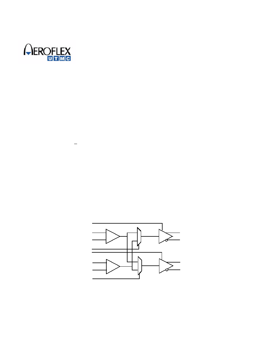
Figure 1a. UT54LVDM228 Crosspoint Switch Block Diagram
(Partial - see Page 2 for complete diagram)
Out1+
En1
In1+
+
-
1
0
1
0
Out 2+
Sel1
En2
In2+
Sel2
+
-
In1-
Out1-
Out 2-
In2-
相关PDF资料 |
PDF描述 |
|---|---|
| 5962R0621302KXC | 1-OUTPUT 40 W DC-DC REG PWR SUPPLY MODULE |
| 5962R9319302KXC | 2-OUTPUT 60 W DC-DC REG PWR SUPPLY MODULE |
| 5962R9316202KXC | 1-OUTPUT 60 W DC-DC REG PWR SUPPLY MODULE |
| 5962R9316102KXC | 1-OUTPUT 65 W DC-DC REG PWR SUPPLY MODULE |
| 5962R0722601VZA | SERIAL INPUT LOADING, 12.5 us SETTLING TIME, 12-BIT DAC, CDSO10 |
相关代理商/技术参数 |
参数描述 |
|---|---|
| 5962F0253201VXC | 制造商:STMicroelectronics 功能描述:LDO Regulator Neg -1.2V to -9.5V 2A 16-Pin CFLAT |
| 5962F0253402VYA | 制造商:STMicroelectronics 功能描述:LDO Regulator Pos 2.5V 3A 3-Pin SMD |
| 5962F0253501VSA | 制造商:STMicroelectronics 功能描述:FLIGHT MODE FIXED VOLTAGE VREG - Bulk |
| 5962F0254501VZA | 功能描述:运算放大器 - 运放 RoHS:否 制造商:STMicroelectronics 通道数量:4 共模抑制比(最小值):63 dB 输入补偿电压:1 mV 输入偏流(最大值):10 pA 工作电源电压:2.7 V to 5.5 V 安装风格:SMD/SMT 封装 / 箱体:QFN-16 转换速度:0.89 V/us 关闭:No 输出电流:55 mA 最大工作温度:+ 125 C 封装:Reel |
| 5962F0254601VPA | 功能描述:运算放大器 - 运放 RoHS:否 制造商:STMicroelectronics 通道数量:4 共模抑制比(最小值):63 dB 输入补偿电压:1 mV 输入偏流(最大值):10 pA 工作电源电压:2.7 V to 5.5 V 安装风格:SMD/SMT 封装 / 箱体:QFN-16 转换速度:0.89 V/us 关闭:No 输出电流:55 mA 最大工作温度:+ 125 C 封装:Reel |
发布紧急采购,3分钟左右您将得到回复。