- 您现在的位置:买卖IC网 > PDF目录67346 > 5962F9467602VPX (INTERSIL CORP) VIDEO AMPLIFIER PDF资料下载
参数资料
| 型号: | 5962F9467602VPX |
| 厂商: | INTERSIL CORP |
| 元件分类: | 音频/视频放大 |
| 英文描述: | VIDEO AMPLIFIER |
| 文件页数: | 4/11页 |
| 文件大小: | 132K |
| 代理商: | 5962F9467602VPX |
2
Typical Applications
Optimum Feedback Resistor
The enclosed plots of inverting and non-inverting frequency
response illustrate the performance of the HS-1100RH in
various gains. Although the bandwidth dependency on
closed loop gain isn’t as severe as that of a voltage
feedback amplifier, there can be an appreciable decrease
in bandwidth at higher gains. This decrease may be
minimized by taking advantage of the current feedback
amplifier’s unique relationship between bandwidth and RF.
All current feedback amplifiers require a feedback resistor,
even for unity gain applications, and RF, in conjunction with
the internal compensation capacitor, sets the dominant
pole of the frequency response. Thus, the amplifier’s
bandwidth is inversely proportional to RF. The HS-1100RH
design is optimized for a 510
RF at a gain of +1.
Decreasing RF in a unity gain application decreases
stability, resulting in excessive peaking and overshoot. At
higher gains the amplifier is more stable, so RF can be
decreased in a trade-off of stability for bandwidth.
The table below lists recommended RF values for various
gains, and the expected bandwidth.
PC Board Layout
The frequency response of this amplier depends greatly on
the amount of care taken in designing the PC board. The
use of low inductance components such as chip
resistors and chip capacitors is strongly recommended,
while a solid ground plane is a must!
Attention should be given to decoupling the power supplies.
A large value (10
F) tantalum in parallel with a small value
(0.1
F) chip capacitor works well in most cases.
Terminated microstrip signal lines are recommended at the
input and output of the device. Capacitance directly on the
output must be minimized, or isolated as discussed in the
next section.
Care must also be taken to minimize the capacitance to
ground seen by the amplier’s inverting input (-IN). The
larger this capacitance, the worse the gain peaking, resulting
in pulse overshoot and possible instability. To this end, it is
recommended that the ground plane be removed under
traces connected to -IN, and connections to -IN should be
kept as short as possible.
An example of a good high frequency layout is the
Evaluation Board shown in Figure 2.
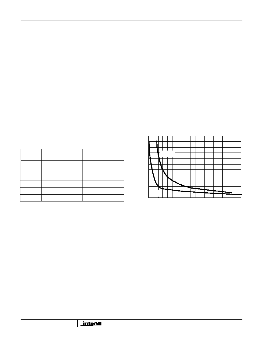
Driving Capacitive Loads
Capacitive loads, such as an A/D input, or an improperly
terminated transmission line will degrade the amplier’s
phase margin resulting in frequency response peaking and
possible oscillations. In most cases, the oscillation can be
avoided by placing a resistor (RS) in series with the output
prior to the capacitance.
Figure 1 details starting points for the selection of this
resistor. The points on the curve indicate the RS and CL
combinations for the optimum bandwidth, stability, and
settling time, but experimental ne tuning is recommended.
Picking a point above or to the right of the curve yields an
overdamped response, while points below or left of the curve
indicate areas of underdamped performance.
RS and CL form a low pass network at the output, thus
limiting system bandwidth well below the amplier bandwidth
of 850MHz. By decreasing RS as CL increases (as
illustrated in the curves), the maximum bandwidth is
obtained without sacricing stability. Even so, bandwidth
does decrease as you move to the right along the curve. For
example, at AV = +1, RS = 50, CL = 30pF, the overall
bandwidth is limited to 300MHz, and bandwidth drops to
100MHz at AV = +1, RS =5, CL = 340pF.
Evaluation Board
The performance of the HS-1100RH may be evaluated using
the HFA11XXEVAL Evaluation Board.
The layout and schematic of the board are shown in
Figure 2. To order evaluation boards, please contact your
local sales ofce.
GAIN
(ACL)
RF ()
BANDWIDTH
(MHz)
-1
430
580
+1
510
850
+2
360
670
+5
150
520
+10
180
240
+19
270
125
R
S
(
)
LOAD CAPACITANCE (pF)
50
45
40
35
30
25
20
15
10
5
0
40
80
120
160
200
240
280
320
360 400
AV = +1
AV = +2
FIGURE 1. RECOMMENDED SERIES OUTPUT RESISTOR vs
LOAD CAPACITANCE
HS-1100RH
相关PDF资料 |
PDF描述 |
|---|---|
| 5962F9669601VXX | 1-CH 8-BIT FLASH METHOD ADC, PARALLEL ACCESS, CDIP28 |
| 5962F9669601VYX | 1-CH 8-BIT FLASH METHOD ADC, PARALLEL ACCESS, CDFP28 |
| 5962F9669601QYX | 1-CH 8-BIT FLASH METHOD ADC, PARALLEL ACCESS, CDFP28 |
| 5962F9669601QXX | 1-CH 8-BIT FLASH METHOD ADC, PARALLEL ACCESS, CDIP28 |
| 5962F9675601VPX | 1 CHANNEL, VIDEO AMPLIFIER, CDIP8 |
相关代理商/技术参数 |
参数描述 |
|---|---|
| 5962F9553601VHA | 功能描述:运算放大器 - 运放 RoHS:否 制造商:STMicroelectronics 通道数量:4 共模抑制比(最小值):63 dB 输入补偿电压:1 mV 输入偏流(最大值):10 pA 工作电源电压:2.7 V to 5.5 V 安装风格:SMD/SMT 封装 / 箱体:QFN-16 转换速度:0.89 V/us 关闭:No 输出电流:55 mA 最大工作温度:+ 125 C 封装:Reel |
| 5962F9553601VPA | 功能描述:运算放大器 - 运放 RoHS:否 制造商:STMicroelectronics 通道数量:4 共模抑制比(最小值):63 dB 输入补偿电压:1 mV 输入偏流(最大值):10 pA 工作电源电压:2.7 V to 5.5 V 安装风格:SMD/SMT 封装 / 箱体:QFN-16 转换速度:0.89 V/us 关闭:No 输出电流:55 mA 最大工作温度:+ 125 C 封装:Reel |
| 5962F9553601VXA | 功能描述:运算放大器 - 运放 RoHS:否 制造商:STMicroelectronics 通道数量:4 共模抑制比(最小值):63 dB 输入补偿电压:1 mV 输入偏流(最大值):10 pA 工作电源电压:2.7 V to 5.5 V 安装风格:SMD/SMT 封装 / 箱体:QFN-16 转换速度:0.89 V/us 关闭:No 输出电流:55 mA 最大工作温度:+ 125 C 封装:Reel |
| 5962F9560401QPA | 功能描述:运算放大器 - 运放 RoHS:否 制造商:STMicroelectronics 通道数量:4 共模抑制比(最小值):63 dB 输入补偿电压:1 mV 输入偏流(最大值):10 pA 工作电源电压:2.7 V to 5.5 V 安装风格:SMD/SMT 封装 / 箱体:QFN-16 转换速度:0.89 V/us 关闭:No 输出电流:55 mA 最大工作温度:+ 125 C 封装:Reel |
| 5962F9560401VPA | 功能描述:运算放大器 - 运放 RoHS:否 制造商:STMicroelectronics 通道数量:4 共模抑制比(最小值):63 dB 输入补偿电压:1 mV 输入偏流(最大值):10 pA 工作电源电压:2.7 V to 5.5 V 安装风格:SMD/SMT 封装 / 箱体:QFN-16 转换速度:0.89 V/us 关闭:No 输出电流:55 mA 最大工作温度:+ 125 C 封装:Reel |
发布紧急采购,3分钟左右您将得到回复。