- 您现在的位置:买卖IC网 > PDF目录91416 > 5962F9683201VCX (INTERSIL CORP) DUAL OP-AMP, CDIP14 PDF资料下载
参数资料
| 型号: | 5962F9683201VCX |
| 厂商: | INTERSIL CORP |
| 元件分类: | 运算放大器 |
| 英文描述: | DUAL OP-AMP, CDIP14 |
| 封装: | CERDIP-14 |
| 文件页数: | 4/4页 |
| 文件大小: | 44K |
| 代理商: | 5962F9683201VCX |
4
All Intersil semiconductor products are manufactured, assembled and tested under ISO9000 quality systems certication.
Intersil semiconductor products are sold by description only. Intersil Corporation reserves the right to make changes in circuit design and/or specifications at any time with-
out notice. Accordingly, the reader is cautioned to verify that data sheets are current before placing orders. Information furnished by Intersil is believed to be accurate and
reliable. However, no responsibility is assumed by Intersil or its subsidiaries for its use; nor for any infringements of patents or other rights of third parties which may result
from its use. No license is granted by implication or otherwise under any patent or patent rights of Intersil or its subsidiaries.
For information regarding Intersil Corporation and its products, see web site http://www.intersil.com
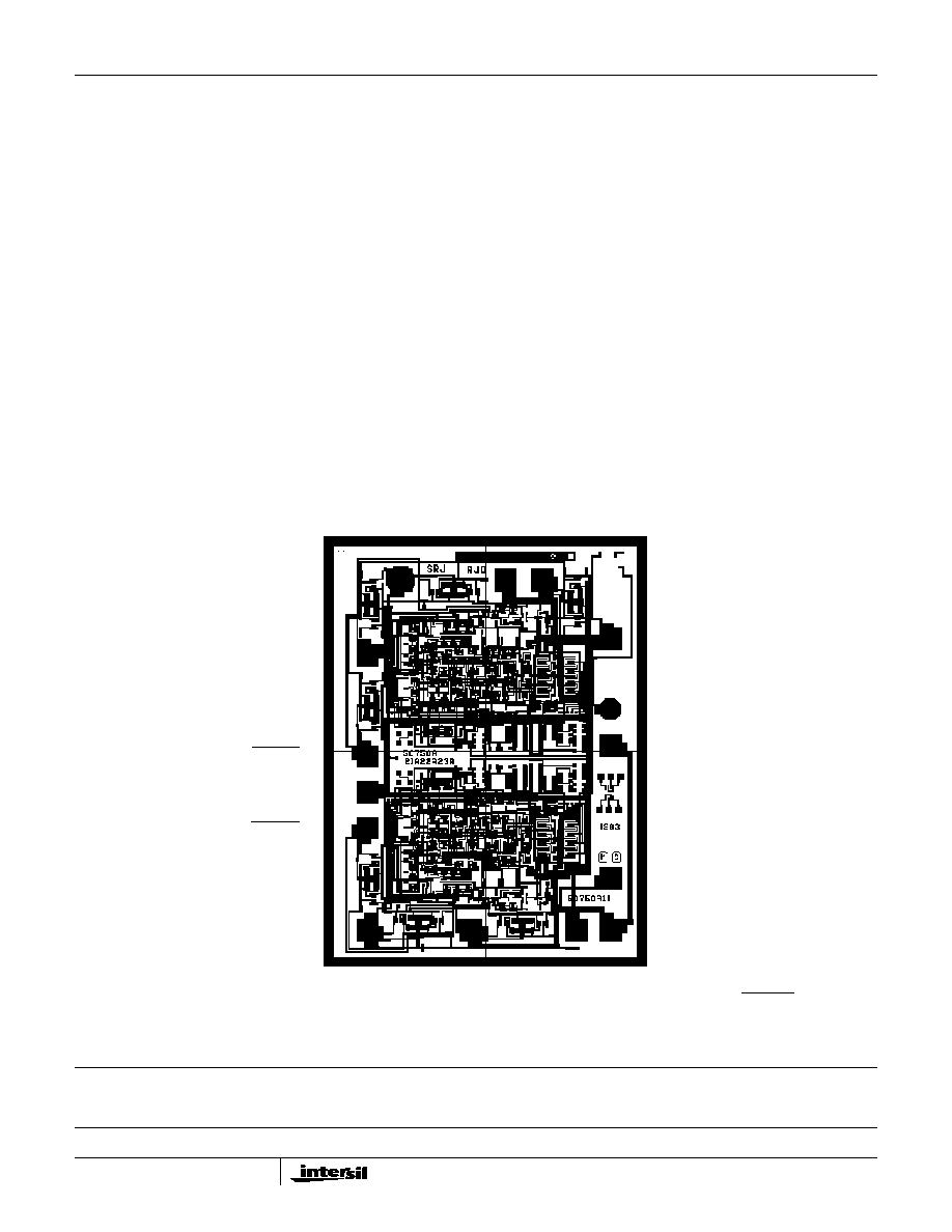
Die Characteristics
DIE DIMENSIONS:
69 mils x 92 mils x 19 mils
±1 mil
1750 x 2330 x 355
m ±25.4m
INTERFACE MATERIALS:
Glassivation:
Type: Nitride
Thickness: 4k
±0.5k
Top Metallization:
Type: Metal 1: AICu(2%)/TiW
Type: Metal 2: AICu(2%)
Thickness: Metal 1: 8k
±0.4k
Thickness: Metal 2: 16k
±0.8k
Substrate:
UHF-1X, Bonded Wafer, DI
Backside Finish:
Silicon
ASSEMBLY RELATED INFORMATION:
Substrate Potential (Powered Up):
Floating
ADDITIONAL INFORMATION:
Worst Case Current Density:
< 2 x 10⁵ A/cm2
Transistor Count:
150
Metallization Mask Layout
HS-1245RH
NOTE: This is an optional GND pad. Users may set a GND reference, via this pad, to ensure the TTL compatibility of the DISABLE inputs when
using asymmetrical supplies (e.g., V+ = 10V, V- = 0V). See the “Application Information” section for details.
V-
OUT2
+IN1
-IN1
V+
VL
+IN2
OUT1
-IN2
NC
GND (NOTE)
DISABLE1
DISABLE2
V-
HS-1245RH
相关PDF资料 |
PDF描述 |
|---|---|
| 5962F9751201VXX | DUAL OP-AMP, 6000 uV OFFSET-MAX, CDFP18 |
| 5962F9861301VCX | QUAD COMPARATOR, 2000 uV OFFSET-MAX, CDIP14 |
| 5962F9861301VXX | QUAD COMPARATOR, 2000 uV OFFSET-MAX, CDFP14 |
| 5962R9566901VCC | SAMPLE AND HOLD AMPLIFIER, CDIP14 |
| 5962R9569001TCC | QUAD OP-AMP, 8 MHz BAND WIDTH, CDIP14 |
相关代理商/技术参数 |
参数描述 |
|---|---|
| 5962F9861301VCC | 制造商:Intersil Corporation 功能描述: |
| 5962F9861301VHA | 制造商:Intersil Corporation 功能描述:- Bulk |
| 5962F9861301VXC | 制造商:Intersil Corporation 功能描述: |
| 5962F9865102QYA | 制造商:STMicroelectronics 功能描述:EIA-644LINE DRIVERQUADFLAT16, SOLDER DIP - Bulk |
| 5962F9865102QYC | 制造商:STMicroelectronics 功能描述:EIA-644LINE DRIVERQUADFLAT16, GOLD - Bulk |
发布紧急采购,3分钟左右您将得到回复。