- 您现在的位置:买卖IC网 > PDF目录298413 > 5962G9654203QXX AC SERIES, QUAD 2-INPUT NAND GATE, CDFP14 PDF资料下载
参数资料
| 型号: | 5962G9654203QXX |
| 元件分类: | 门电路 |
| 英文描述: | AC SERIES, QUAD 2-INPUT NAND GATE, CDFP14 |
| 封装: | CERAMIC, BOTTOM BRAZED, DFP-14 |
| 文件页数: | 3/8页 |
| 文件大小: | 177K |
| 代理商: | 5962G9654203QXX |
3
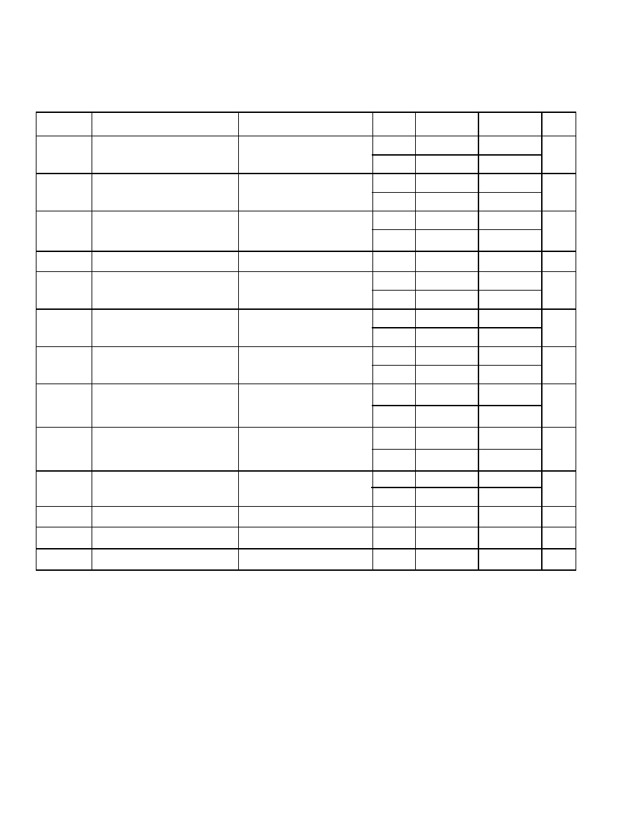
DC ELECTRICAL CHARACTERISTICS FOR THE UT54ACS132E7
( VDD = 3.0V to 5.5V; VSS = 0V
6; -55
°C < T
C < +125°C)
Notes:
1. Functional tests are conducted in accordance with MIL-STD-883 with the following input test conditions: VIH = VIH(min) + 20%, - 0%; VIL = VIL(max) + 0%, - 50%,
as specified herein, for TTL, CMOS, or Schmitt compatible inputs. Devices may be tested using any input voltage within the above specified range, but are guaranteed
to VIH(min) and VIL(max).
2. Supplied as a design limit but not guaranteed or tested.
3. Per MIL-PRF-38535, for current density
≤5.0E5 amps/cm2, the maximum product of load capacitance (per output buffer) times frequency should not exceed 3,765pF/
MHz.
4. Not more than one output may be shorted at a time for maximum duration of one second.
5. Capacitance measured for initial qualification and when design changes may affect the value. Capacitance is measured between the designated terminal and VSS at
frequency of 1MHz and a signal amplitude of 50mV rms maximum.
6. Maximum allowable relative shift equals 50mV.
7. All specifications valid for radiation dose
≤ 1E6 rads(Si) per MIL-STD-883 Method 1019 Condition B.
8. Power dissipation specified per switching output.
9. This value is guaranteed based on characterization data, but not tested.
SYMBOL
Description
CONDITION
VDD
MIN
MAX
UNIT
VT+
Schmitt trigger positive-going
threshold 1
3.0V
2.1
V
5.5V
3.85
VT-
Schmitt trigger negative-going
threshold 1
3.0V
0.9
V
5.5V
1.65
VH
Hysteresis2
(VT+ - VT-)
3.0V
0.3
1.2
V
4.5V
.6
1.5
IIN
Input leakage current
VIN = VDD or VSS
5.5V
-1
1
A
VOL
Low-level output voltage 3
IOL = 100A
3.0V
0.25
V
4.5V
0.25
VOH
High-level output voltage 3
IOH = -100A
3.0V
2.75
V
4.5V
4.25
IOS
Short-circuit output current 2 ,4
VO = VDD and VSS
3.0V
-100
100
mA
5.5V
-200
200
IOL
Low level output current9
VIN = VDD or VSS
VOL = 0.4V
3.0V
6
mA
5.5V
8
IOH
High level output current9
VIN = VDD or VSS
VOH = VDD-0.4V
3.0V
-6
mA
5.5V
-8
Ptotal
Power dissipation 2, 8
CL = 50pF
5.5V
3.0V
1.9
0.76
mW/
MHz
IDDQ
Quiescent Supply Current
VIN = VDD or VSS
5.5V
10
A
CIN
Input capacitance 5
= 1MHz
0V
15
pF
COUT
Output capacitance 5
= 1MHz
0V
15
pF
相关PDF资料 |
PDF描述 |
|---|---|
| 5962G9654203VXA | AC SERIES, QUAD 2-INPUT NAND GATE, CDFP14 |
| 5962G9654203VXX | AC SERIES, QUAD 2-INPUT NAND GATE, CDFP14 |
| 5962H9654202QXA | AC SERIES, QUAD 2-INPUT NAND GATE, CDFP14 |
| 5962R9654203VXA | AC SERIES, QUAD 2-INPUT NAND GATE, CDFP14 |
| 5962R9654203VXC | AC SERIES, QUAD 2-INPUT NAND GATE, CDFP14 |
相关代理商/技术参数 |
参数描述 |
|---|---|
| 5962H94A0305QXC | 制造商: 功能描述: 制造商:undefined 功能描述: |
| 5962H9853701 | 制造商: 功能描述: 制造商:undefined 功能描述: |
| 5962L0051502VHA | 制造商:Analog Devices 功能描述:AEROSPACE 7NS SINGLE COMPARATOR - Trays |
| 5962L0052401VGA | 功能描述:校验器 IC RoHS:否 制造商:STMicroelectronics 产品: 比较器类型: 通道数量: 输出类型:Push-Pull 电源电压-最大:5.5 V 电源电压-最小:1.1 V 补偿电压(最大值):6 mV 电源电流(最大值):1350 nA 响应时间: 最大工作温度:+ 125 C 安装风格:SMD/SMT 封装 / 箱体:SC-70-5 封装:Reel |
| 5962L0052401VHA | 功能描述:校验器 IC RoHS:否 制造商:STMicroelectronics 产品: 比较器类型: 通道数量: 输出类型:Push-Pull 电源电压-最大:5.5 V 电源电压-最小:1.1 V 补偿电压(最大值):6 mV 电源电流(最大值):1350 nA 响应时间: 最大工作温度:+ 125 C 安装风格:SMD/SMT 封装 / 箱体:SC-70-5 封装:Reel |
发布紧急采购,3分钟左右您将得到回复。