- 您现在的位置:买卖IC网 > PDF目录293971 > 5962H0151601QXC 8K X 8 OTPROM, 55 ns, CDIP28 PDF资料下载
参数资料
| 型号: | 5962H0151601QXC |
| 元件分类: | PROM |
| 英文描述: | 8K X 8 OTPROM, 55 ns, CDIP28 |
| 封装: | 0.600 X 1.400 INCH, 2.54 MM PITCH, CERAMIC, DIP-28 |
| 文件页数: | 4/11页 |
| 文件大小: | 152K |
| 代理商: | 5962H0151601QXC |
2
DEVICE OPERATION
The UT28F64LV has three control inputs: Chip Enable (CE),
Program Enable (PE), and Output Enable (OE); thirteen address
inputs, A(12:0); and eight bidirectional data lines, DQ(7:0). CE
is the device enable input that controls chip selection, active, and
standby modes. AssertingCE causes I DD to rise to its active value
and decodes the thirteen address inputs to select one of 8,192
words in the memory. PE controls program and read operations.
During a read cycle, OE must be asserted to enable the outputs.
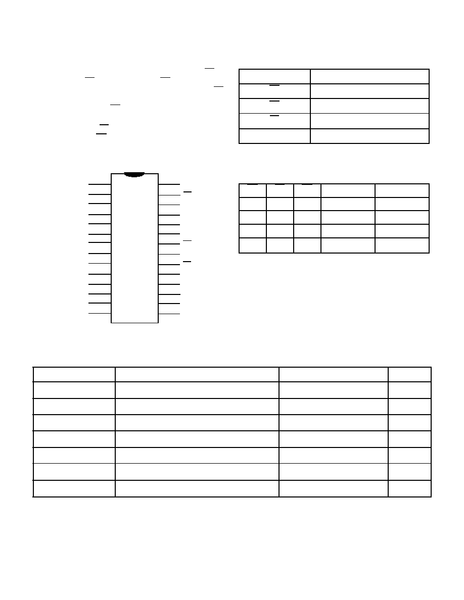
PIN NAMES
Table 1. Device Operation Truth Table
1
Notes:
1. “X” is defined as a “don’t care” condition.
2. Device active; outputs disabled.
ABSOLUTE MAXIMUM RATINGS 1
(Referenced to VSS)
Notes:
1. Stresses outside the listed absolute maximum ratings may cause permanent damage to the device. This is a stress rating only, and functional operation of the
device at these or any other conditions beyond limits indicated in the operational sections of this specification is not recommended. Exposure to
absolute maximum rating conditions for extended periods may affect device reliability.
2. Test per MIL-STD-883, Method 1012, infinite heat sink.
NC
A12
A7
A6
A5
A4
A3
A2
A1
A0
DQ0
DQ1
DQ2
VSS
VDD
PE
NC
A8
A9
A11
OE
A10
CE
DQ7
DQ6
DQ5
DQ4
DQ3
PIN CONFIGURATION
1
2
3
4
5
6
7
8
9
10
11
12
13
14
28
27
26
25
24
23
22
21
20
19
18
17
16
15
A(12:0)
Address
CE
Chip Enable
OE
Output Enable
PE
Program Enable
DQ(7:0)
Data Input/Data Output
OE
PE
CE
I/O MODE
MODE
X
1
Three-state
Standby
0
1
0
Data Out
Read
1
0
Data In
Program
1
0
Three-state
Read 2
SYMBOL
PARAMETER
LIMITS
UNITS
V
DD
DC supply voltage
-0.3 to 7.0
V
VI/O
Voltage on any pin
-0.5 to (VDD + 0.5)
V
TSTG
Storage temperature
-65 to +150
°C
P
D
Maximum power dissipation
1.5
W
TJ
Maximum junction temperature
+175
°C
Θ
JC
Thermal resistance, junction-to-case 2
3.3
°C/W
I
DC input current
±10
mA
相关PDF资料 |
PDF描述 |
|---|---|
| 5962G9651403QXC | AC SERIES, QUAD 2-INPUT NOR GATE, CDFP14 |
| 5962G9654203QXA | AC SERIES, QUAD 2-INPUT NAND GATE, CDFP14 |
| 5962G9655103VXX | ACT SERIES, DUAL 4 LINE TO 1 LINE MULTIPLEXER, TRUE OUTPUT, CDFP16 |
| 5962R0150201VYC | 32-BIT, 12 MHz, RISC PROCESSOR, CPGA144 |
| 5962R0150202VYX | 16-BIT, 16 MHz, RISC PROCESSOR, QFP132 |
相关代理商/技术参数 |
参数描述 |
|---|---|
| 5962H94A0305QXC | 制造商: 功能描述: 制造商:undefined 功能描述: |
| 5962H9853701 | 制造商: 功能描述: 制造商:undefined 功能描述: |
| 5962L0051502VHA | 制造商:Analog Devices 功能描述:AEROSPACE 7NS SINGLE COMPARATOR - Trays |
| 5962L0052401VGA | 功能描述:校验器 IC RoHS:否 制造商:STMicroelectronics 产品: 比较器类型: 通道数量: 输出类型:Push-Pull 电源电压-最大:5.5 V 电源电压-最小:1.1 V 补偿电压(最大值):6 mV 电源电流(最大值):1350 nA 响应时间: 最大工作温度:+ 125 C 安装风格:SMD/SMT 封装 / 箱体:SC-70-5 封装:Reel |
| 5962L0052401VHA | 功能描述:校验器 IC RoHS:否 制造商:STMicroelectronics 产品: 比较器类型: 通道数量: 输出类型:Push-Pull 电源电压-最大:5.5 V 电源电压-最小:1.1 V 补偿电压(最大值):6 mV 电源电流(最大值):1350 nA 响应时间: 最大工作温度:+ 125 C 安装风格:SMD/SMT 封装 / 箱体:SC-70-5 封装:Reel |
发布紧急采购,3分钟左右您将得到回复。