- 您现在的位置:买卖IC网 > PDF目录208010 > 5962H0521402VXX 200 MHz, OTHER CLOCK GENERATOR, CDFP48 PDF资料下载
参数资料
| 型号: | 5962H0521402VXX |
| 元件分类: | XO, clock |
| 英文描述: | 200 MHz, OTHER CLOCK GENERATOR, CDFP48 |
| 封装: | CERAMIC, DFP-48 |
| 文件页数: | 1/23页 |
| 文件大小: | 174K |
| 代理商: | 5962H0521402VXX |
1
IN
DEVELOPMENT
FEATURES:
+3.3V Core Power Supply
+2.5V or +3.3V Clock Output Power Supply
- Independent Clock Output Bank Power Supplies
Output frequency range: 6 MHz to 200 MHz
Output-output skew < 100 ps
Cycle-cycle jitter < 100 ps
± 2% maximum output duty cycle
Eight LVTTL outputs with selectable drive strength
Selectable positive- or negative-edge synchronization
Selectable phase-locked loop (PLL) frequency range and
lock indicator
Phase adjustments in 625 to 1300 ps steps up to ± 7.8 ns
(1-6,8,10,12) x multiply and (1/2,1/4) x divide ratios
Compatible with Spread-Spectrum reference clocks
Power-down mode
Selectable reference input divider
Radiation performance
- Total-dose tolerance: 300 krad (Si) and 1 Mrad (Si)
- SEL Immune to a LET of 109 MeV-cm2/mg
- SEU Immune to a LET of 109 MeV-cm2/mg
- SET: Contact factory for details
Military temperature range: -55oC to +125oC
Packaging options:
- 48-Lead Ceramic Flatpack
Standard Microcircuit Drawing: 5962-05214
- QML-Q and QML-V compliant part
INTRODUCTION:
The UT7R995/UT7R995C is a low-voltage, low-power, eight-
output, 6-to-200 MHz clock driver. It features output phase
programmability which is necessary to optimize the timing of
high-performance microprocessor and communication sys-
tems.
The user programs both the frequency and the phase of the out-
put banks through nF[1:0] and DS[1:0] pins. The adjustable
phase feature allows the user to skew the outputs to lead or lag
the reference clock. Connect any one of the outputs to the
feedback input to achieve different reference frequency multi-
plication and division ratios.
The devices also feature split output bank power supplies that
enable banks 1 & 2, bank 3, and bank 4 to operate at a different
power supply levels. The ternary PE/HD pin controls the syn-
chronization of output signals to either the rising or the falling
edge of the reference clock and selects the drive strength of the
output buffers. The UT7R995 and UT7R995C both interface
to a digital clock while the UT7R995C will also interface to a
quartz crystal.
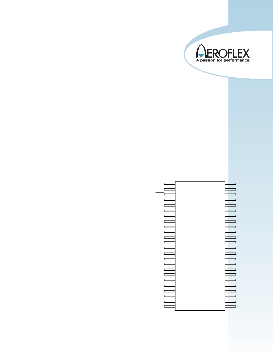
Figure 1. 48-Lead Ceramic Flatpack Pin Description
1
2
3
4
5
6
7
8
9
10
11
12
13
14
15
16
17
18
19
20
21
22
23
24
48
47
46
45
44
43
42
41
40
39
38
37
36
35
34
33
32
31
30
29
28
27
26
25
4F0
4F1
sOE
PD/DIV
PE/HD
VDD
VDDQ3
3Q1
3Q0
VSS
VDD
FB
VDD
VSS
2Q1
2Q0
VDDQ1
LOCK
VSS
DS0
DS1
1F0
3F1
3F0
FS
VSS
VDDQ4
4Q1
4Q0
VSS
VDD
XTAL1
NC/XTAL2
VDD
VSS
1Q1
1Q0
VDDQ1
VSS
TEST
2F1
2F0
1F1
UT7R995
&
UT7R995C
Standard Products
UT7R995 & UT7R995C RadClockTM
RadHard 2.5V/3.3V 200MHz High-Speed
Multi-phase PLL Clock Buffer
Advanced Data Sheet
November 30, 2005
相关PDF资料 |
PDF描述 |
|---|---|
| 5962F0521404VXA | 200 MHz, OTHER CLOCK GENERATOR, CDFP48 |
| 5962H0521404VXA | 200 MHz, OTHER CLOCK GENERATOR, CDFP48 |
| 514DCAXXXXXXBAG | 250 MHz, OTHER CLOCK GENERATOR, PDSO6 |
| 514ECCXXXXXXAAGR | 125 MHz, OTHER CLOCK GENERATOR, PDSO6 |
| 514KCAXXXXXXBAGR | 250 MHz, OTHER CLOCK GENERATOR, PDSO6 |
相关代理商/技术参数 |
参数描述 |
|---|---|
| 5962H94A0305QXC | 制造商: 功能描述: 制造商:undefined 功能描述: |
| 5962H9853701 | 制造商: 功能描述: 制造商:undefined 功能描述: |
| 5962L0051502VHA | 制造商:Analog Devices 功能描述:AEROSPACE 7NS SINGLE COMPARATOR - Trays |
| 5962L0052401VGA | 功能描述:校验器 IC RoHS:否 制造商:STMicroelectronics 产品: 比较器类型: 通道数量: 输出类型:Push-Pull 电源电压-最大:5.5 V 电源电压-最小:1.1 V 补偿电压(最大值):6 mV 电源电流(最大值):1350 nA 响应时间: 最大工作温度:+ 125 C 安装风格:SMD/SMT 封装 / 箱体:SC-70-5 封装:Reel |
| 5962L0052401VHA | 功能描述:校验器 IC RoHS:否 制造商:STMicroelectronics 产品: 比较器类型: 通道数量: 输出类型:Push-Pull 电源电压-最大:5.5 V 电源电压-最小:1.1 V 补偿电压(最大值):6 mV 电源电流(最大值):1350 nA 响应时间: 最大工作温度:+ 125 C 安装风格:SMD/SMT 封装 / 箱体:SC-70-5 封装:Reel |
发布紧急采购,3分钟左右您将得到回复。