- 您现在的位置:买卖IC网 > PDF目录97787 > 5962P0052401QPA (NATIONAL SEMICONDUCTOR CORP) COMPARATOR, 4000 uV OFFSET-MAX, 200 ns RESPONSE TIME, CDIP8 PDF资料下载
参数资料
| 型号: | 5962P0052401QPA |
| 厂商: | NATIONAL SEMICONDUCTOR CORP |
| 元件分类: | 比较器 |
| 英文描述: | COMPARATOR, 4000 uV OFFSET-MAX, 200 ns RESPONSE TIME, CDIP8 |
| 封装: | CERDIP-8 |
| 文件页数: | 2/28页 |
| 文件大小: | 674K |
| 代理商: | 5962P0052401QPA |
第1页当前第2页第3页第4页第5页第6页第7页第8页第9页第10页第11页第12页第13页第14页第15页第16页第17页第18页第19页第20页第21页第22页第23页第24页第25页第26页第27页第28页
7.0 LM311 Typical Performance Characteristics (Continued)
8.0 Application Hints
8.1 CIRCUIT TECHNIQUES FOR AVOIDING
OSCILLATIONS IN COMPARATOR APPLICATIONS
When a high-speed comparator such as the LM111 is used
with fast input signals and low source impedances, the out-
put response will normally be fast and stable, assuming that
the power supplies have been bypassed (with 0.1 F disc
capacitors), and that the output signal is routed well away
from the inputs (pins 2 and 3) and also away from pins 5 and
6.
However, when the input signal is a voltage ramp or a slow
sine wave, or if the signal source impedance is high (1 k
to
100 k
), the comparator may burst into oscillation near the
crossing-point. This is due to the high gain and wide band-
width of comparators like the LM111. To avoid oscillation or
instability in such a usage, several precautions are recom-
mended, as shown in
Figure 1 below.
1.
The trim pins (pins 5 and 6) act as unwanted auxiliary
inputs. If these pins are not connected to a trim-pot, they
should be shorted together. If they are connected to a
trim-pot, a 0.01 F capacitor C1 between pins 5 and 6
will minimize the susceptibility to AC coupling. A smaller
capacitor is used if pin 5 is used for positive feedback as
in
Figure 1.
2.
Certain sources will produce a cleaner comparator out-
put waveform if a 100 pF to 1000 pF capacitor C2 is
connected directly across the input pins.
3.
When the signal source is applied through a resistive
network, R
S, it is usually advantageous to choose an RS'
of substantially the same value, both for DC and for
dynamic (AC) considerations. Carbon, tin-oxide, and
metal-film resistors have all been used successfully in
comparator input circuitry. Inductive wirewound resistors
are not suitable.
4.
When comparator circuits use input resistors (eg. sum-
ming resistors), their value and placement are particu-
larly important. In all cases the body of the resistor
should be close to the device or socket. In other words
there should be very little lead length or printed-circuit
foil run between comparator and resistor to radiate or
pick up signals. The same applies to capacitors, pots,
etc. For example, if R
S=10 k, as little as 5 inches of
lead between the resistors and the input pins can result
in oscillations that are very hard to damp. Twisting these
input leads tightly is the only (second best) alternative to
placing resistors close to the comparator.
5.
Since feedback to almost any pin of a comparator can
result in oscillation, the printed-circuit layout should be
engineered thoughtfully. Preferably there should be a
groundplane under the LM111 circuitry, for example, one
side of a double-layer circuit card. Ground foil (or, posi-
tive supply or negative supply foil) should extend be-
tween the output and the inputs, to act as a guard. The
foil connections for the inputs should be as small and
compact as possible, and should be essentially sur-
rounded by ground foil on all sides, to guard against
capacitive coupling from any high-level signals (such as
the output). If pins 5 and 6 are not used, they should be
shorted together. If they are connected to a trim-pot, the
trim-pot should be located, at most, a few inches away
from the LM111, and the 0.01 F capacitor should be
installed. If this capacitor cannot be used, a shielding
printed-circuit foil may be advisable between pins 6 and
7. The power supply bypass capacitors should be lo-
cated within a couple inches of the LM111. (Some other
comparators require the power-supply bypass to be lo-
cated immediately adjacent to the comparator.)
6.
It is a standard procedure to use hysteresis (positive
feedback) around a comparator, to prevent oscillation,
and to avoid excessive noise on the output because the
comparator is a good amplifier for its own noise. In the
circuit of
Figure 2, the feedback from the output to the
positive input will cause about 3 mV of hysteresis. How-
ever, if R
S is larger than 100, such as 50 k, it would
not be reasonable to simply increase the value of the
positive feedback resistor above 510 k
. The circuit of
Figure 3 could be used, but it is rather awkward. See the
notes in paragraph 7 below.
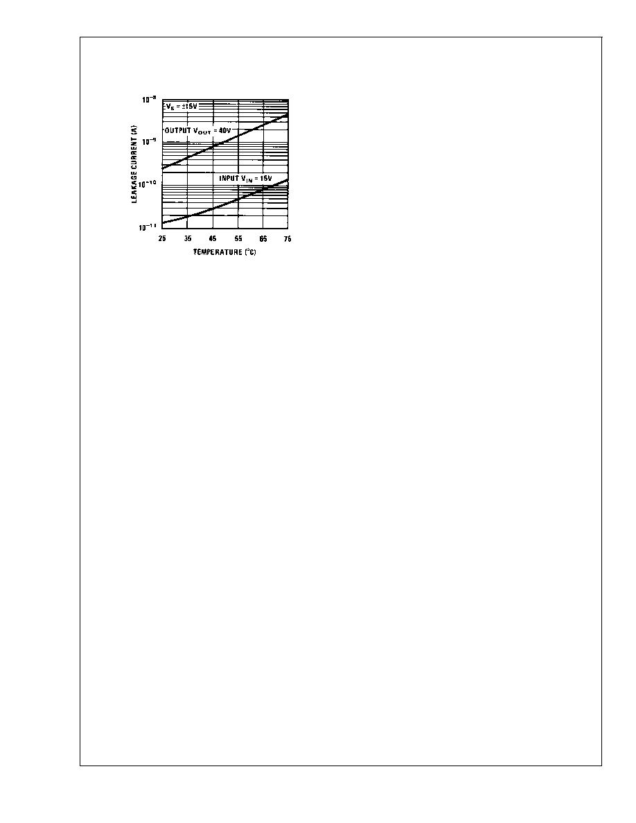
Leakage Currents
DS005704-72
LM1
1
1/LM21
1/LM31
1
www.national.com
10
相关PDF资料 |
PDF描述 |
|---|---|
| 5962P0052401QZA | COMPARATOR, 4000 uV OFFSET-MAX, 200 ns RESPONSE TIME, CDSO10 |
| 5962P0052401VGA | COMPARATOR, 4000 uV OFFSET-MAX, 200 ns RESPONSE TIME, MBCY8 |
| 5962P0052401VZA | COMPARATOR, 4000 uV OFFSET-MAX, 200 ns RESPONSE TIME, CDSO10 |
| 5962P0052401VHA | COMPARATOR, 4000 uV OFFSET-MAX, 200 ns RESPONSE TIME, CDFP10 |
| 5962P9853901VGA | OP-AMP, 6000 uV OFFSET-MAX, 15 MHz BAND WIDTH, MBCY8 |
相关代理商/技术参数 |
参数描述 |
|---|---|
| 5962P9951701VXA | 功能描述:线性稳压器 - 标准 RoHS:否 制造商:STMicroelectronics 输出类型: 极性: 输出电压:1.8 V 输出电流:150 mA 负载调节: 最大输入电压:5.5 V 线路调整率: 最大工作温度:+ 125 C 安装风格:SMD/SMT 封装 / 箱体:SOT-323-5L |
| 5962P9951708VXA | 制造商:Texas Instruments 功能描述:5962P9951708VXA - Rail/Tube |
| 5962R0050101VXA | 功能描述:基准电压& 基准电流 RoHS:否 制造商:STMicroelectronics 产品:Voltage References 拓扑结构:Shunt References 参考类型:Programmable 输出电压:1.24 V to 18 V 初始准确度:0.25 % 平均温度系数(典型值):100 PPM / C 串联 VREF - 输入电压(最大值): 串联 VREF - 输入电压(最小值): 分流电流(最大值):60 mA 最大工作温度:+ 125 C 封装 / 箱体:SOT-23-3L 封装:Reel |
| 5962R0051501VHA | 制造商:Analog Devices 功能描述:COMPARATOR SGL 5V/10V 10PIN FLATPACK - Rail/Tube |
| 5962R0051501VPA |
发布紧急采购,3分钟左右您将得到回复。