- 您现在的位置:买卖IC网 > PDF目录293971 > 5962R9215311VTX 32K X 8 STANDARD SRAM, 55 ns, CDFP36 PDF资料下载
参数资料
| 型号: | 5962R9215311VTX |
| 元件分类: | SRAM |
| 英文描述: | 32K X 8 STANDARD SRAM, 55 ns, CDFP36 |
| 封装: | 0.700 X 1 INCH, 0.050 INCH PITCH, TOP BRAZED, CERAMIC, FP-36 |
| 文件页数: | 9/15页 |
| 文件大小: | 144K |
| 代理商: | 5962R9215311VTX |
3
WRITE CYCLE
A combination of W less than VIL(max), E1 less than VIL(max),
and E2 greater than VIH(min) defines a write cycle. The state of
G is a “don’t care” for a write cycle. The outputs are placed in
the high-impedance state when either G is greater than
VIH(min), or when W is less than VIL(max).
Write Cycle 1, the Write Enable-controlled Access shown in
figure 4a, is defined by a write terminated by W going high, with
E1 and E2 still active. The write pulse width is defined by tWLWH
when the write is initiated by W, and by tETWH when the write
is initiated by the latter of E1 or E2. Unless the outputs have
been previously placed in the high-impedance state by G, the
user must wait tWLQZ before applying data to the eight
bidirectional pins DQ(7:0) to avoid bus contention.
Write Cycle 2, the Chip Enable-controlled Access shown in
figure 4b, is defined by a write terminated by the latter of E1 or
E2 going inactive. The write pulse width is defined by tWLEF
when the write is initiated by W, and by tETEF when the write
is initiated by the latter of E1 or E2 going active. For the W
initiated write, unless the outputs have been previously placed
in the high-impedance state by G, the user must wait tWLQZ
before applying data to the eight bidirectional pins DQ(7:0) to
avoid bus contention.
RADIATION HARDNESS
The UT7156 SRAM incorporates special design and layout
features which allow operation in high-level radiation
environments.
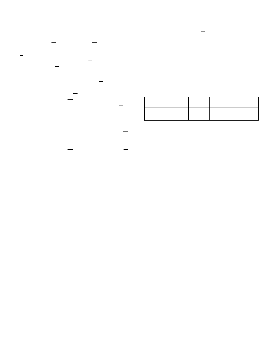
Table 2. Radiation Hardness
Design Specifications1
Notes:
1. The SRAM will not latchup during radiation exposure under recommended
operating conditions.
2. 10% worst case particle environment, Geosynchronous orbit, 0.025 mils of
Aluminum.
Total Dose
1.0E6
rads(Si)
Error Rate2
1.0E-10
Errors/Bit-Day
相关PDF资料 |
PDF描述 |
|---|---|
| 5962G9215309VMX | 32K X 8 STANDARD SRAM, 55 ns, CDIP28 |
| 5962F9215315VMC | 32K X 8 STANDARD SRAM, 70 ns, CDIP28 |
| 5962H9215315QMA | 32K X 8 STANDARD SRAM, 70 ns, CDIP28 |
| 5962R9581901QQX | 24 I/O, PIA-GENERAL PURPOSE, CDIP40 |
| 59K16A-102T4 | CABLE TERMINATED, FEMALE, RF CONNECTOR, CRIMP, JACK |
相关代理商/技术参数 |
参数描述 |
|---|---|
| 5962R9325801VCA | 制造商:Analog Devices 功能描述:OP AMP QUAD GP 18V 14CDIP - Rail/Tube |
| 5962R9325801VDA | 制造商:Analog Devices 功能描述:OP AMP QUAD GP 18V 14PIN FLATPACK - Rail/Tube |
| 5962R9452602VGA | 功能描述:校验器 IC RoHS:否 制造商:STMicroelectronics 产品: 比较器类型: 通道数量: 输出类型:Push-Pull 电源电压-最大:5.5 V 电源电压-最小:1.1 V 补偿电压(最大值):6 mV 电源电流(最大值):1350 nA 响应时间: 最大工作温度:+ 125 C 安装风格:SMD/SMT 封装 / 箱体:SC-70-5 封装:Reel |
| 5962R9452602VPA | 功能描述:校验器 IC Lo PWR Lo Offset RoHS:否 制造商:STMicroelectronics 产品: 比较器类型: 通道数量: 输出类型:Push-Pull 电源电压-最大:5.5 V 电源电压-最小:1.1 V 补偿电压(最大值):6 mV 电源电流(最大值):1350 nA 响应时间: 最大工作温度:+ 125 C 安装风格:SMD/SMT 封装 / 箱体:SC-70-5 封装:Reel |
| 5962R9452603VGA | 功能描述:校验器 IC RoHS:否 制造商:STMicroelectronics 产品: 比较器类型: 通道数量: 输出类型:Push-Pull 电源电压-最大:5.5 V 电源电压-最小:1.1 V 补偿电压(最大值):6 mV 电源电流(最大值):1350 nA 响应时间: 最大工作温度:+ 125 C 安装风格:SMD/SMT 封装 / 箱体:SC-70-5 封装:Reel |
发布紧急采购,3分钟左右您将得到回复。