- 您现在的位置:买卖IC网 > PDF目录97787 > 5962R9863702QCA (NATIONAL SEMICONDUCTOR CORP) OP-AMP, 3000 uV OFFSET-MAX, CDFP14 PDF资料下载
参数资料
| 型号: | 5962R9863702QCA |
| 厂商: | NATIONAL SEMICONDUCTOR CORP |
| 元件分类: | 运算放大器 |
| 英文描述: | OP-AMP, 3000 uV OFFSET-MAX, CDFP14 |
| 封装: | CERAMIC, FP-14 |
| 文件页数: | 4/20页 |
| 文件大小: | 758K |
| 代理商: | 5962R9863702QCA |
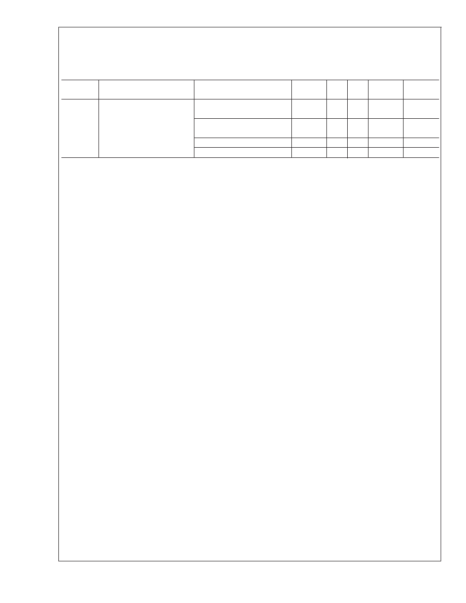
LM108A Rad Hard — Electrical Characteristics (Continued)
The following conditions apply to all the following parameters, unless otherwise specified.
DC:
±V
CC = ±20V, VCM = 0V, RS =50
Symbol
Parameter
Conditions
Notes
Min
Max
Units
Sub-
groups
I
IO
Input Offset Current
+V
CC = 35V, -VCC = -5V,
V
CM = -15V
0.5
nA
1
+V
CC = 5V, -VCC = -35V,
V
CM = -15V
0.5
nA
1
0.5
nA
1
+V
CC = +5V, -VCC = -5V
0.5
nA
1
Note 2: Parameters have only been entered in the LM108 / LM108A column if different from LM108RH
Note 3: Absolute Maximum Ratings indicate limits beyond which damage to the device may occur. Operating Ratings indicate conditions for which the device is
functional, but do not guarantee specific performance limits. For guaranteed specifications and test conditions, see the Electrical Characteristics. The guaranteed
specifications apply only for the test conditions listed. Some performance characteristics may degrade when the device is not operated under the listed test
conditions.
Note 4: The maximum power dissipation must be derated at elevated temperatures and is dictated by TJmax (maximum junction temperature), θJA (package
junction to ambient thermal resistance), and TA (ambient temperature). The maximum allowable power dissipation at any temperature is PDmax=(TJmax - TA)/θJA
or the number given in the Absolute Maximum Ratings, whichever is lower.
Note 5: The inputs are shunted with back-to-back diodes for over voltage protection. Therefore, excessive current will flow if a differential input voltage in excess
of 1V is applied between the inputs unless some limiting resistance is used.
Note 6: For supply voltages less than ±20V, the absolute maximum input voltage is equal to the supply voltage.
Note 7: This rating is ±1.0V unless resistances of 2K Ohms or greater are inserted in series with the inputs to limit current in the input shunt diodes to the maximum
allowable value..
Note 8: Human body model, 1.5 k
in series with 100 pF.
Note 9: Calculated parameter
Note 10: Datalog reading in K = V/mV
Note 11: Pre and post irradiation limits are identical to those listed under AC and DC electrical characteristics except as listed in the Post Radiation Limits Table.
These parts may be dose rate sensitive in a space environment and demonstrate enhanced low dose rate effect. Radiation end point limits for the noted parameters
are guaranteed only for the conditions as specified in MIL-STD-883, Method 1019.5.
Note 12: Parameter tested Go-No-Go
Note 13: Guaranteed parameter not tested.
Note 14: Calculated parameter for Class “S” only
LM108/LM108AQML
www.national.com
12
相关PDF资料 |
PDF描述 |
|---|---|
| 5962R9863702VCA | OP-AMP, 3000 uV OFFSET-MAX, CDFP14 |
| 5962R9863702VPA | OP-AMP, 3000 uV OFFSET-MAX, CDIP8 |
| 5962R9863702QZA | OP-AMP, 3000 uV OFFSET-MAX, CDSO10 |
| 5962R9863702VZA | OP-AMP, 3000 uV OFFSET-MAX, CDSO10 |
| 5962R9863901V2X | OP-AMP, 400 uV OFFSET-MAX, CQCC20 |
相关代理商/技术参数 |
参数描述 |
|---|---|
| 5962R9863702QZA | 制造商:Analog Devices 功能描述: |
| 5962R9863702VZA | 制造商:Analog Devices 功能描述: |
| 5962R9863901VGA | 制造商:Analog Devices 功能描述:OP AMP SGL GP 20V 8PIN TO-99 - Rail/Tube |
| 5962R9863901VHA | 制造商:Analog Devices 功能描述:OP AMP SGL GP 20V 10PIN FLATPACK - Rail/Tube |
| 5962R9864602VXA |
发布紧急采购,3分钟左右您将得到回复。