- 您现在的位置:买卖IC网 > PDF目录91420 > 5FL2CZ47A 5 A, 300 V, SILICON, RECTIFIER DIODE PDF资料下载
参数资料
| 型号: | 5FL2CZ47A |
| 元件分类: | 整流器 |
| 英文描述: | 5 A, 300 V, SILICON, RECTIFIER DIODE |
| 封装: | 12-10C1A, 3 PIN |
| 文件页数: | 1/5页 |
| 文件大小: | 397K |
| 代理商: | 5FL2CZ47A |
5DL2CZ47A,5FL2CZ47A,5GL2CZ47A
2006-11-08
1
TOSHIBA HIGH EFFICIENCY DIODE STACK (HED) SILICON EPITAXIAL TYPE
5DL2CZ47A, 5FL2CZ47A, 5GL2CZ47A
SWITCHING MODE POWER SUPPLY APPLICATION
CONVERTER & CHOPPER APPLICATION
Repetitive Peak Reverse Voltage
: VRRM = 200 V, 300 V, 400V
Average Output Rectified Current
: IO = 5 A
Ultra Fast Reverse-Recovery Time
: trr = 35 ns (Max)
Low Switching Losses and Output Noise.
ABSOLUTE MAXIMUM RATINGS (Ta = 25°C)
CHARACTERISTIC
SYMBOL
RATING
UNIT
5DL2CZ47A
200
5FL2CZ47A
300
Repetitive Peak
Reverse Voltage
5GL2CZ47A
VRRM
400
V
Average Output Rectified Current
IO
5
A
25 (50Hz)
Peak One Cycle Surge Forward
Current (Sin Wave)
IFSM
27.5 (60Hz)
A
Junction Temperature
Tj
40~150
°C
Storage Temperature Range
Tstg
40~150
°C
Screw Torque
―
0.6
Nm
Note: Using continuously under heavy loads (e.g. the application of high temperature/current/voltage and the
significant change in temperature, etc.) may cause this product to decrease in the reliability significantly even
if the operating conditions (i.e. operating temperature/current/voltage, etc.) are within the absolute maximum
ratings.
Please design the appropriate reliability upon reviewing the Toshiba Semiconductor Reliability Handbook
(“Handling Precautions”/Derating Concept and Methods) and individual reliability data (i.e. reliability test report
and estimated failure rate, etc).
ELECTRICAL CHARACTERISTICS (Ta = 25°C)
CHARACTERISTIC
SYMBOL
TEST CONDITION
TYP.
MAX
UNIT
5DL2CZ47A
―
0.98
5FL2CZ47A
―
1.3
Peak Forward
Voltage
(Note 1)
5GL2CZ47A
VFM
IFM = 2.5A
―
1.8
V
5DL2CZ47A
―
10
5FL2CZ47A
―
10
Repetitive Peak
Reverse Current
(Note 1)
5GL2CZ47A
IRRM
VRRM = Rated
―
50
μA
Reverse Recovery Time
(Note 1)
trr
IF = 2A, di / dt = 20A / μs
―
35
ns
Forward Recovery Time
(Note 1)
tfr
IF = 1A
―
100
ns
Thermal Resistance
Rth (jc)
Total DC, Junction to Case
―
3.8
°C / W
Note 1: A value applied to one cell.
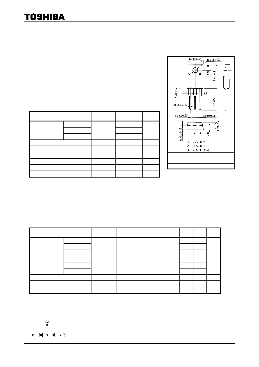
POLARITY
JEDEC
―
JEITA
―
TOSHIBA
1210C1A
Weight: 2.0 g
Unit: mm
相关PDF资料 |
PDF描述 |
|---|---|
| 5DL2CZ47A | 5 A, 200 V, SILICON, RECTIFIER DIODE |
| 5FWJ2C42 | 5 A, 30 V, SILICON, RECTIFIER DIODE, TO-220AB |
| 5FWJ2C48M | 2.5 A, 30 V, SILICON, RECTIFIER DIODE |
| 5FWJ2C48M | 5 A, 30 V, SILICON, RECTIFIER DIODE |
| 5FWJ2CZ47M | 5 A, 30 V, SILICON, RECTIFIER DIODE |
相关代理商/技术参数 |
参数描述 |
|---|---|
| 5FL2CZ47A(F) | 制造商:Toshiba America Electronic Components 功能描述: 制造商:Toshiba America Electronic Components 功能描述:Diode Switching 300V 5A 3-Pin(3+Tab) TO-220NIS |
| 5FLR | 制造商:Molex 功能描述: |
| 5FN9695 | 制造商:Vishay Dale 功能描述: |
| 5FRP9C | 制造商:HELLERMANNTYTON 功能描述:SPIRALWRAP 1'' FR POLY 制造商:HellermannTyton 功能描述:Spiralwrap 1'' Diameter - Flame Retardant Polyethylene, Natural, 100ft/reel |
| 5FS1 | 制造商:Fairchild Semiconductor Corporation 功能描述: |
发布紧急采购,3分钟左右您将得到回复。