- 您现在的位置:买卖IC网 > PDF目录19554 > 5M1270ZF324C5N (Altera)IC MAX V CPLD 1270 LE 324-FBGA PDF资料下载
参数资料
| 型号: | 5M1270ZF324C5N |
| 厂商: | Altera |
| 文件页数: | 22/30页 |
| 文件大小: | 0K |
| 描述: | IC MAX V CPLD 1270 LE 324-FBGA |
| 产品培训模块: | Max V Overview |
| 特色产品: | MAX? V CPLDs |
| 标准包装: | 84 |
| 系列: | MAX® V |
| 可编程类型: | 系统内可编程 |
| 最大延迟时间 tpd(1): | 6.2ns |
| 电压电源 - 内部: | 1.71 V ~ 1.89 V |
| 逻辑元件/逻辑块数目: | 1270 |
| 宏单元数: | 980 |
| 输入/输出数: | 271 |
| 工作温度: | 0°C ~ 85°C |
| 安装类型: | 表面贴装 |
| 封装/外壳: | 324-LBGA |
| 供应商设备封装: | 324-FBGA(19x19) |
| 包装: | 托盘 |
第1页第2页第3页第4页第5页第6页第7页第8页第9页第10页第11页第12页第13页第14页第15页第16页第17页第18页第19页第20页第21页当前第22页第23页第24页第25页第26页第27页第28页第29页第30页
�� �
�
�3–22�
�Chapter� 3:� DC� and� Switching� Characteristics� for� MAX� V� Devices�
�Timing� Model� and� Specifications�
��5M1270Z� device.�
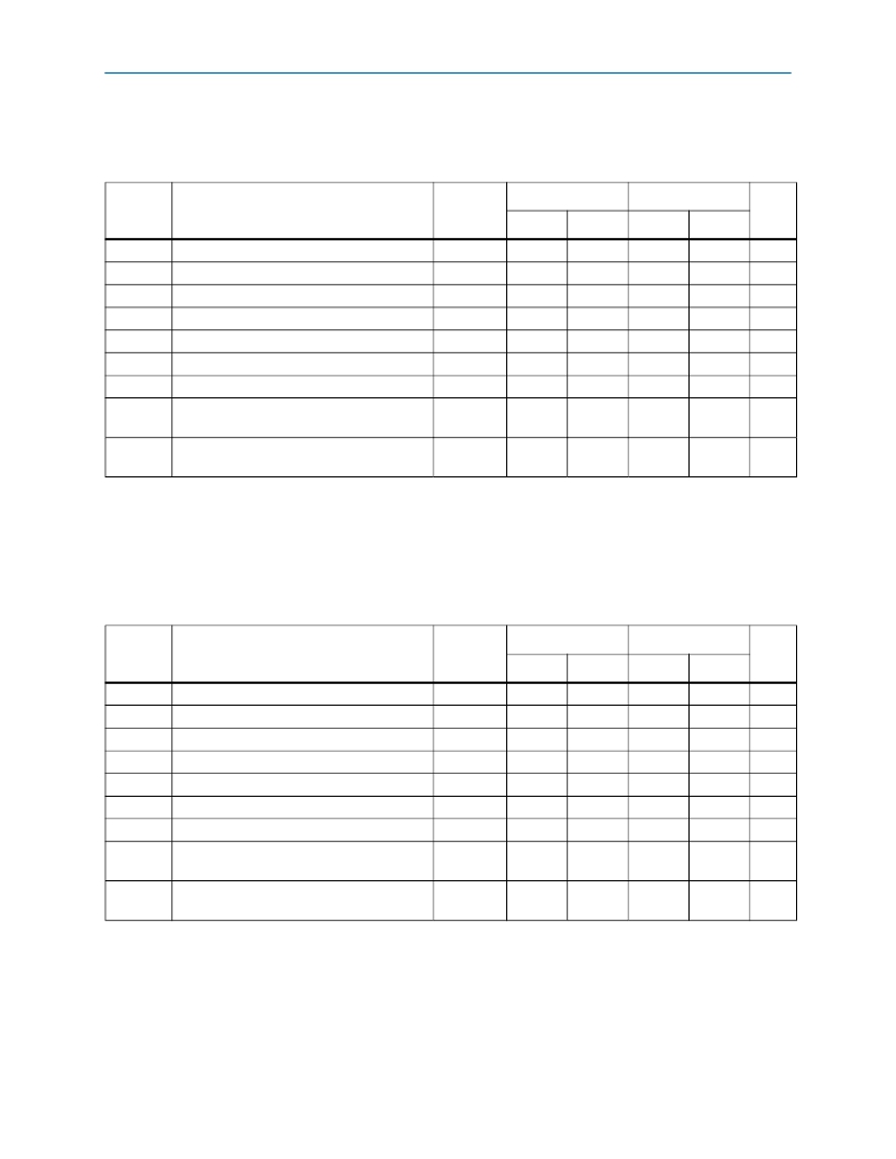
�Table� 3–30.� Global� Clock� External� I/O� Timing� Parameters� for� the� 5M1270Z� Device� (Note� 1)� ,� (2)�
�C4�
�C5,� I5�
�Symbol�
�Parameter�
�Condition�
�Unit�
�Min�
�Max�
�Min�
�Max�
�t� PD1�
�t� PD2�
�t� SU�
�t� H�
�t� CO�
�t� CH�
�t� CL�
�t� CNT�
�f� CNT�
�Worst� case� pin-to-pin� delay� through� one� LUT�
�Best� case� pin-to-pin� delay� through� one� LUT�
�Global� clock� setup� time�
�Global� clock� hold� time�
�Global� clock� to� output� delay�
�Global� clock� high� time�
�Global� clock� low� time�
�Minimum� global� clock� period� for� 16-bit�
�counter�
�Maximum� global� clock� frequency� for� 16-bit�
�counter�
�10� pF�
�10� pF�
�—�
�—�
�10� pF�
�—�
�—�
�—�
�—�
�—�
�—�
�1.5�
�0�
�2.0�
�216�
�216�
�4.0�
�—�
�9.1�
�4.8�
�—�
�—�
�6.0�
�—�
�—�
�—�
�247.5�
�—�
�—�
�1.9�
�0�
�2.0�
�266�
�266�
�5.0�
�—�
�11.2�
�5.9�
�—�
�—�
�7.4�
�—�
�—�
�—�
�201.1�
�ns�
�ns�
�ns�
�ns�
�ns�
�ps�
�ps�
�ns�
�MHz�
��(1)� The� maximum� frequency� is� limited� by� the� I/O� standard� on� the� clock� input� pin.� The� 16-bit� counter� critical� delay� performs� faster� than� this� global�
�clock� input� pin� maximum� frequency.�
�(2)� Only� applicable� to� the� F324� package� of� the� 5M1270Z� device.�
��Table� 3–31.� Global� Clock� External� I/O� Timing� Parameters� for� the� 5M2210Z� Device� (Note� 1)�
�C4�
�C5,� I5�
�Symbol�
�Parameter�
�Condition�
�Unit�
�Min�
�Max�
�Min�
�Max�
�t� PD1�
�t� PD2�
�t� SU�
�t� H�
�t� CO�
�t� CH�
�t� CL�
�t� CNT�
�f� CNT�
�Worst� case� pin-to-pin� delay� through� one� LUT�
�Best� case� pin-to-pin� delay� through� one� LUT�
�Global� clock� setup� time�
�Global� clock� hold� time�
�Global� clock� to� output� delay�
�Global� clock� high� time�
�Global� clock� low� time�
�Minimum� global� clock� period� for� 16-bit�
�counter�
�Maximum� global� clock� frequency� for� 16-bit�
�counter�
�10� pF�
�10� pF�
�—�
�—�
�10� pF�
�—�
�—�
�—�
�—�
�—�
�—�
�1.5�
�0�
�2.0�
�216�
�216�
�4.0�
�—�
�9.1�
�4.8�
�—�
�—�
�6.0�
�—�
�—�
�—�
�247.5�
�—�
�—�
�1.9�
�0�
�2.0�
�266�
�266�
�5.0�
�—�
�11.2�
�5.9�
�—�
�—�
�7.4�
�—�
�—�
�—�
�201.1�
�ns�
�ns�
�ns�
�ns�
�ns�
�ps�
�ps�
�ns�
�MHz�
��(1)� The� maximum� frequency� is� limited� by� the� I/O� standard� on� the� clock� input� pin.� The� 16-bit� counter� critical� delay� performs� faster� than� this� global�
�clock� input� pin� maximum� frequency.�
��May� 2011�
�Altera� Corporation�
�相关PDF资料 |
PDF描述 |
|---|---|
| ABM40DRSN-S288 | CONN EDGECARD EXTEND 80POS .156 |
| EGM36DTBT-S273 | CONN EDGECARD 72POS R/A .156 SLD |
| FCE17C37SA440 | CONN D-SUB RCPT 37POS R/A GOLD |
| EYM36DTAT-S273 | CONN EDGECARD 72POS R/A .156 SLD |
| 5M570ZF256I5N | IC MAX V CPLD 570 LE 256-FBGA |
相关代理商/技术参数 |
参数描述 |
|---|---|
| 5M1270ZF324I5 | 制造商:Altera Corporation 功能描述:IC CPLD 980MC 6.2NS 324FBGA 制造商:Altera Corporation 功能描述:IC MAX V CPLD |
| 5M1270ZF324I5N | 功能描述:CPLD - 复杂可编程逻辑器件 CPLD - MAX V 980 Macro 271 IOs RoHS:否 制造商:Lattice 系列: 存储类型:EEPROM 大电池数量:128 最大工作频率:333 MHz 延迟时间:2.7 ns 可编程输入/输出端数量:64 工作电源电压:3.3 V 最大工作温度:+ 90 C 最小工作温度:0 C 封装 / 箱体:TQFP-100 |
| 5M1270ZF64A4N | 制造商:ALTERA 制造商全称:Altera Corporation 功能描述:MAX V Device Handbook |
| 5M1270ZF64I4N | 制造商:ALTERA 制造商全称:Altera Corporation 功能描述:MAX V Device Handbook |
| 5M1270ZM64A4N | 制造商:ALTERA 制造商全称:Altera Corporation 功能描述:MAX V Device Handbook |
发布紧急采购,3分钟左右您将得到回复。