- 您现在的位置:买卖IC网 > PDF目录369228 > 66158-001 (MICROPAC INDUSTRIES INC) MTP-FC (12) FANOUT ASSY MM, 1 M PDF资料下载
参数资料
| 型号: | 66158-001 |
| 厂商: | MICROPAC INDUSTRIES INC |
| 元件分类: | 光电耦合器 |
| 英文描述: | MTP-FC (12) FANOUT ASSY MM, 1 M |
| 中文描述: | 1 CHANNEL TRANSISTOR OUTPUT OPTOCOUPLER |
| 封装: | TO-46, 4 PIN |
| 文件页数: | 1/2页 |
| 文件大小: | 85K |
| 代理商: | 66158-001 |
MICROPAC INDUSTRIES, INC.
OPTOELECTRONIC PRODUCTS DIVISION
725 E. Walnut St., Garland, TX 75040
(972) 272-3571
Fax (972) 487-6918
www.micropac.com
E-MAIL:
optosales@micropac.com
3 - 46
66158
SINGLE CHANNEL OPTOCOUPLER
DIRECT REPLACEMENT FOR 3C92C
Mii
OPTOELECTRONIC PRODUCTS
DIVISION
REVISION B
12/29/00
Features:
High Reliability
Base lead eliminated for improved noise immunity
Rugged package
Stability over wide temperature
+500V electrical isolation
Applications:
Eliminate ground loops
Level shifting
Line receiver
Switching power supplies
Motor control
DESCRIPTION
The
66158
contains a gallium arsenide infrared LED optically coupled to a silicon planar phototransistor. The optocoupler
is built on a TO-46 header. The collector of the phototransistor is electrically connected to the case. This optocoupler is
capable of transmitting signals between two galvanic sources. The potential difference between transmitter and receiver
should not go over the maximum isolation voltage. The internal base connection has been eliminated for improved noise
immunity.
ABSOLUTE MAXIMUM RATINGS
Input to Output Voltage.......................................................................................................................................................500V
Emitter-Collector Voltage........................................................................................................................................................7V
Collector-Emitter Voltage (value applies to emitter-base open-circuited & the input-diode equal to zero) ........................60V
Reverse Input Voltage ...........................................................................................................................................................7V
Input Diode Continuous Forward Current at (or below) 65°C Free-Air Temperature (see note 1) .................................50mA
Peak Forward Input Current (value applies for tw
<
1
μ
s, PRR
<
300 pps) .....................................................................500mA
Continuous Collector Current............................................................................................................................................50mA
Continuous Transistor Power Dissipation at (or below) 25°C Free-Air Temperature (see Note 2) ..............................230mW
Storage Temperature........................................................................................................................................-65°C to +150°C
Operating Free-Air Temperature Range..........................................................................................................-55°C to +125°C
Lead Solder Temperature (10 seconds max.) ................................................................................................................ 260°C
Notes:
1. Derate linearly to 125°C free-air temperature at the rate of 0.67 mA/
°
C above 65°C.
2. Derate linearly to 125°C free-air temperature at the rate of 2.3 mW/
°
C.
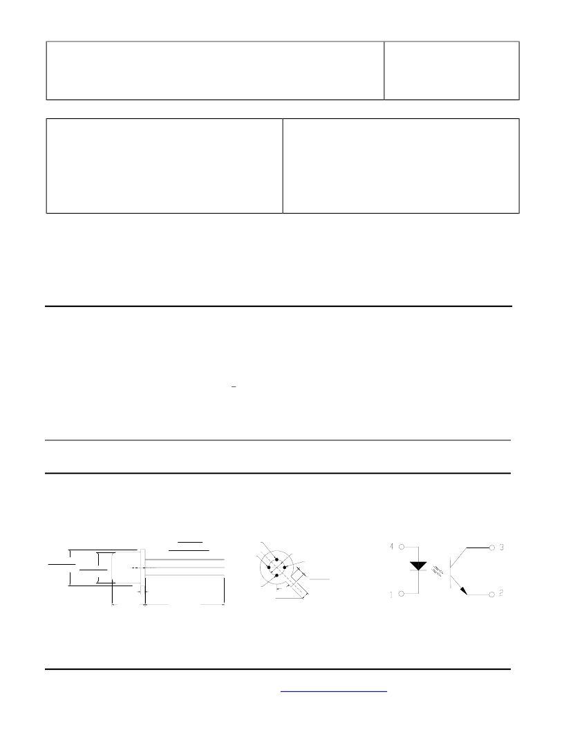
Package Dimensions
Schematic Diagram
1
2
3
45°
DIMENSIONS ARE IN INCHES (MILLIMETERS)
0.030 (0.76) MAX
0.178 (4.52)
0.195 (4.95)
0.230 (5.84)
0.209 (5.31)
4 LEADS
0.019 (0.48)
0.016 (0.41)
0.100[2.54]
0.50 [12.70] MIN
0.210 [5.34]
0.170 [4.32]
ANODE
0.048 [1.22]
0.028 [0.71]
0.046 [1.17]
0.036 [0.91]
COLLECTOR
EMMITTER
CATHODE
4
相关PDF资料 |
PDF描述 |
|---|---|
| 66158-011 | FC/UPC-FC/UPC CRAMIC TERMSNGL MDE CBL SMPLX PVC 2M |
| 66158 | SINGLE CHANNEL OPTOCOUPLER DIRECT REPLACEMENT FOR 3C92C |
| 66158-101 | SINGLE CHANNEL OPTOCOUPLER DIRECT REPLACEMENT FOR 3C92C |
| 66163-001 | CONNECTOR ACCESSORY |
| 66163-011 | SINGLE CHANNEL OPTOCOUPLERS DIRECT REPLACEMENT FOR 3C91C |
相关代理商/技术参数 |
参数描述 |
|---|---|
| 66158-011 | 制造商:MII 制造商全称:MII 功能描述:SINGLE CHANNEL OPTOCOUPLER DIRECT REPLACEMENT FOR 3C92C |
| 66158-101 | 制造商:MII 制造商全称:MII 功能描述:SINGLE CHANNEL OPTOCOUPLER DIRECT REPLACEMENT FOR 3C92C |
| 66159 | 功能描述:VINYL MAT STATFREE DK BLU 18"X50 制造商:desco 系列:Statfree B2?? 零件状态:有效 垫类型:桌子,工作台卷筒 形状:矩形 长度:50'(15.24m) 宽度:1.5'(0.46m) 厚度:0.06"(1.52mm) 颜色:绿 材料:热塑塑胶 特性:耗散 包括:- 标准包装:1 |
| 66-15959-1 | 制造商: 功能描述: 制造商:undefined 功能描述: |
| 6615-99-712-8804 | 制造商:undefined 功能描述: |
发布紧急采购,3分钟左右您将得到回复。