- 您现在的位置:买卖IC网 > PDF目录174148 > 6N137#520 1 CHANNEL LOGIC OUTPUT OPTOCOUPLER, 10 Mbps PDF资料下载
参数资料
| 型号: | 6N137#520 |
| 元件分类: | 光电耦合器 |
| 英文描述: | 1 CHANNEL LOGIC OUTPUT OPTOCOUPLER, 10 Mbps |
| 封装: | 0.300 INCH, SURFACE MOUNT, DIP-8 |
| 文件页数: | 14/22页 |
| 文件大小: | 213K |
| 代理商: | 6N137#520 |
21
Propagation Delay, Pulse-Width Distortion and Propagation
Delay Skew
Propagation delay is a gure of merit which describes
how quickly a logic signal propagates through a sys-
tem. The propagation delay from low to high (t
PLH
) is the
amount of time required for an input signal to propagate
to the output, causing the output to change from low to
high. Similarly, the propagation delay from high to low
(t
PHL
) is the amount of time required for the input signal
to propagate to the output causing the output to change
from high to low (see Figure 8).
Pulse-width distortion (PWD) results when t
PLH
and t
PHL
dier in value. PWD is dened as the dierence be-
tween t
PLH
and t
PHL
and often determines the maximum
data rate capability of a transmission system. PWD can
be expressed in percent by dividing the PWD (in ns) by
the minimum pulse width (in ns) being transmitted. Typi-
cally, PWD on the order of 20-30% of the minimum pulse
width is tolerable; the exact gure depends on the par-
ticular application (RS232, RS422, T-l, etc.).
Propagation delay skew, t
PSK
, is an important parameter to
consider in parallel data applications where synchroniza-
tion of signals on parallel data lines is a concern. If the
parallel data is being sent through a group of optocou-
plers, dierences in propagation delays will cause the
data to arrive at the outputs of the optocouplers at dier-
ent times. If this dierence in propagation delays is large
enough, it will determine the maximum rate at which
parallel data can be sent through the optocouplers.
Propagation delay skew is dened as the dierence be-
tween the minimum and maximum propagation delays,
either t
PLH
or t
PHL
, for any given group of optocouplers
which are operating under the same conditions (i.e., the
same drive current, supply voltage, output load, and op-
erating temperature). As illustrated in Figure 19, if the in-
puts of a group of optocouplers are switched either ON
or OFF at the same time, t
PSK
is the dierence between
the shortest propagation delay, either t
PLH
or t
PHL
, and the
longest propagation delay, either t
PLH
or t
PHL
.
As mentioned earlier, t
PSK
can determine the maximum
parallel data transmission rate. Figure 20 is the timing
diagram of a typical parallel data application with both
the clock and the data lines being sent through opto-
couplers. The gure shows data and clock signals at the
inputs and outputs of the optocouplers. To obtain the
maximum data transmission rate, both edges of the
clock signal are being used to clock the data; if only one
edge were used, the clock signal would need to be twice
as fast.
Propagation delay skew represents the uncertainty of
where an edge might be after being sent through an
optocoupler. Figure 20 shows that there will be uncer-
tainty in both the data and the clock lines. It is important
that these two areas of uncertainty not overlap, other-
wise the clock signal might arrive before all of the data
outputs have settled, or some of the data outputs may
start to change before the clock signal has arrived. From
these considerations, the absolute minimum pulse width
that can be sent through optocouplers in a parallel appli-
cation is twice t
PSK
. A cautious design should use a slightly
longer pulse width to ensure that any additional uncer-
tainty in the rest of the circuit does not cause a problem.
The t
PSK
specied optocouplers oer the advantages of
guaranteed specications for propagation delays, pulse-
width distortion and propagation delay skew over the
recommended temperature, input current, and power
supply ranges.
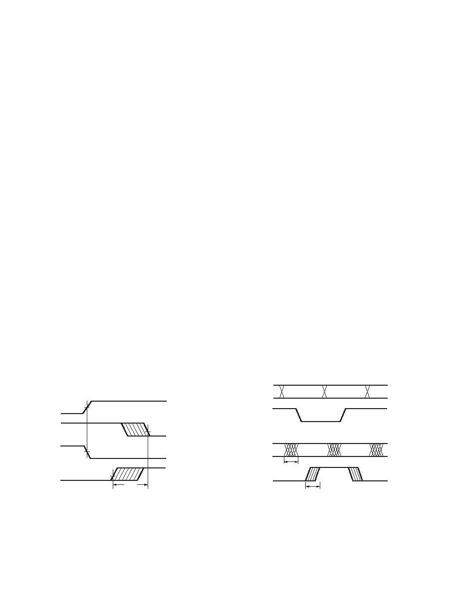
Figure 19. Illustration of propagation delay skew - t
PSK.
Figure 20. Parallel data transmission example.
50%
1.5 V
I F
VO
50%
I F
VO
tPSK
1.5 V
DATA
t PSK
INPUTS
CLOCK
DATA
OUTPUTS
CLOCK
t PSK
相关PDF资料 |
PDF描述 |
|---|---|
| HCPL-2630-520 | 2 CHANNEL LOGIC OUTPUT OPTOCOUPLER, 10 Mbps |
| HCPL-4504#300E | 1 CHANNEL LOGIC OUTPUT OPTOCOUPLER |
| HCPL-5200 | 1 CHANNEL LOGIC OUTPUT OPTOCOUPLER, 5 Mbps |
| HCPL-5230#100 | 2 CHANNEL LOGIC OUTPUT OPTOCOUPLER, 5 Mbps |
| HCPL-5230#300 | 2 CHANNEL LOGIC OUTPUT OPTOCOUPLER, 5 Mbps |
相关代理商/技术参数 |
参数描述 |
|---|---|
| 6N137-520E | 功能描述:高速光耦合器 10 Mb/s 5000Vrms RoHS:否 制造商:Avago Technologies 电流传递比: 最大波特率: 最大正向二极管电压:1.75 V 最大反向二极管电压:5 V 最大功率耗散:40 mW 最大工作温度:+125 C 最小工作温度:- 40 C 封装 / 箱体:SOIC-5 封装:Tube |
| 6N137-560 | 功能描述:OPTOCOUPLER(10MBD) T/R+VDE 制造商:broadcom limited 系列:- 零件状态:在售 通道数:1 输入 - 输入侧 1/输入侧 2:1/0 电压 - 隔离:3750Vrms 共模瞬态抗扰度(最小值):1kV/μs 输入类型:DC 输出类型:开集,肖特基箝位 电流 - 输出/通道:50mA 数据速率:10MBd 传播延迟 tpLH / tpHL(最大值):75ns,75ns 上升/下降时间(典型值):24ns,10ns 电压 - 正向(Vf)(典型值):1.8V(最大) 电流 - DC 正向(If):20mA 电压 - 电源:4.5 V ~ 5.5 V 工作温度:-40°C ~ 85°C 标准包装:1,000 |
| 6N137-560E | 功能描述:高速光耦合器 10 Mb/s 3750Vrms RoHS:否 制造商:Avago Technologies 电流传递比: 最大波特率: 最大正向二极管电压:1.75 V 最大反向二极管电压:5 V 最大功率耗散:40 mW 最大工作温度:+125 C 最小工作温度:- 40 C 封装 / 箱体:SOIC-5 封装:Tube |
| 6N137A | 制造商:Vishay Angstrohm 功能描述:DIP-8 CPLR SNGL 10MBD 1KV/US - 制造商:Vishay Semiconductors 功能描述:DIP-8 CPLR SNGL 10MBD 1KV/US -E3 - Tape and Reel 制造商:Vishay Semiconductors 功能描述:OPTOCOUPLER 1CH 10MBD 8DIP 制造商:Vishay Semiconductors 功能描述:OPTOCOUPLER, LOGIC GATE O/P, 5KV, DIP-8; No. of Channels:1; Isolation Voltage:5kV; Optocoupler Output Type:Logic Gate; Input Current:20mA; Output Voltage:7V; Opto Case Style:DIP; No. of Pins:8 ;RoHS Compliant: Yes |
| 6N137A-X001 | 制造商:Vishay Angstrohm 功能描述:DIP-8 CPLR SNGL 10MBD 1KV/US V 制造商:Vishay Semiconductors 功能描述:DIP-8 CPLR SNGL 10MBD 1KV/US VDE-E3 - Tape and Reel 制造商:Vishay Semiconductors 功能描述:OPTOCOUPLER 1CH 10MBD 8DIP 制造商:Vishay Semiconductors 功能描述:OPTOCOUPLER, LOGIC GATE O/P, 5KV, DIP-8; No. of Channels:1; Isolation Voltage:5kV; Optocoupler Output Type:Logic Gate; Input Current:20mA; Output Voltage:7V; Opto Case Style:DIP; No. of Pins:8 ;RoHS Compliant: Yes |
发布紧急采购,3分钟左右您将得到回复。