- 您现在的位置:买卖IC网 > PDF目录360408 > 74AHC273PWDH (NXP SEMICONDUCTORS) Octal D-type flip-flop with reset; positive-edge trigger PDF资料下载
参数资料
| 型号: | 74AHC273PWDH |
| 厂商: | NXP SEMICONDUCTORS |
| 元件分类: | 通用总线功能 |
| 英文描述: | Octal D-type flip-flop with reset; positive-edge trigger |
| 中文描述: | AHC SERIES, POSITIVE EDGE TRIGGERED D FLIP-FLOP, TRUE OUTPUT, PDSO20 |
| 封装: | 4.40 MM, PLASTIC, SOT-360-1, TSSOP-20 |
| 文件页数: | 2/20页 |
| 文件大小: | 92K |
| 代理商: | 74AHC273PWDH |
1999 Sep 01
2
Philips Semiconductors
Product specification
Octal D-type flip-flop with reset;
positive-edge trigger
74AHC273; 74AHCT273
FEATURES
Ideal buffer for MOS microcontroller or memory
Common clock and master reset
ESD protection:
HBM EIA/JESD22-A114-A exceeds 2000 V
MM EIA/JESD22-A115-A exceeds 200 V
CDM EIA/JESD22-C101 exceeds 1000 V
Balanced propagation delays
All inputs have Schmitt trigger actions
Inputs accepts voltages higher than V
CC
See ‘377’ for clock enable version
See ‘373’ for transparent latch version
See ‘374’ for 3-state version
For AHC only: operates with CMOS input levels
For AHCT only: operates with TTL input levels
Specified from
40 to +85
°
C and
40 to +125
°
C.
DESCRIPTION
The 74AHC/AHCT273 are high-speed Si-gate CMOS
devices and are pin compatible with low power Schottky
TTL (LSTTL). They are specified in compliance with
JEDEC standard no. 7A.
The 74AHC/AHCT273 have eight edge-triggered, D-type
flip-flops with individual D inputs and Q outputs.
Thecommonclock(CP)andmasterreset(MR)inputsload
and reset (clear) all flip-flops simultaneously.
The state of each D input, one set-up time before the
LOW-to-HIGH clock transition, is transferred to the
corresponding output (Q
n
) of the flip-flop.
All outputs will be forced LOW independently of clock or
data inputs by a LOW on the MR input.
The device is useful for applications where the true output
only is required and the clock and master reset are
common to all storage elements.
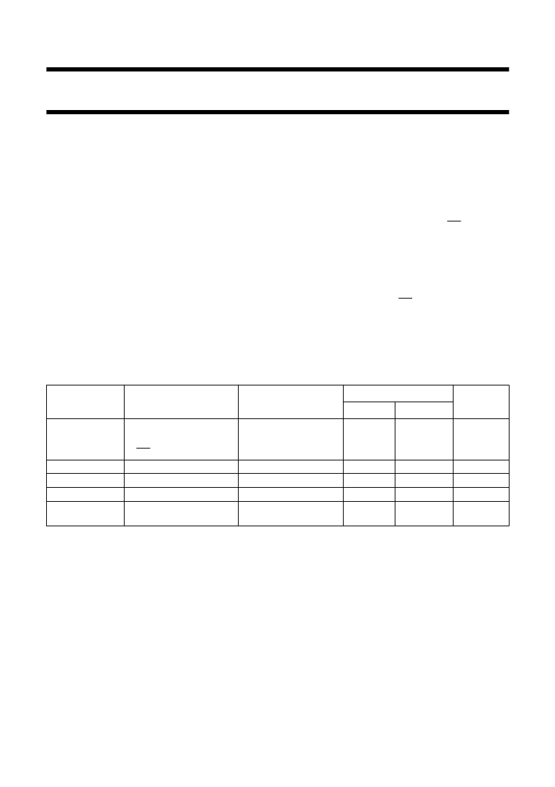
QUICK REFERENCE DATA
Ground = 0 V; T
amb
= 25
°
C; t
r
= t
f
≤
3.0 ns.
Notes
1.
C
PD
is used to determine the dynamic power dissipation (P
D
in
μ
W).
P
D
= C
PD
×
V
CC2
×
f
i
+
∑
(C
L
×
V
CC2
×
f
o
) where:
f
i
= input frequency in MHz;
f
o
= output frequency in MHz;
∑
(C
L
×
V
CC2
×
f
o
) = sum of outputs;
C
L
= output load capacitance in pF;
V
CC
= supply voltage in Volts.
The condition is V
I
= GND to V
CC
.
2.
SYMBOL
PARAMETER
CONDITIONS
TYPICAL
UNIT
AHC
AHCT
t
PHL
/t
PLH
propagation delay
CP to Q
n
MR to Q
n
maximum clock frequency
input capacitance
output capacitance
power dissipation
capacitance
C
L
= 15 pF; V
CC
= 5 V
4.2
3.7
120
3.0
4.0
14.0
4.0
3.9
120
3.0
4.0
18.0
ns
ns
MHz
pF
pF
pF
f
max
C
I
C
O
C
PD
C
L
= 15 pF; V
CC
= 5 V
V
I
= V
CC
or GND
C
L
= 50 pF; f = 1 MHz;
notes 1 and 2
相关PDF资料 |
PDF描述 |
|---|---|
| 74AHCT2G | Dual 2-input OR gate |
| 74AHC2G | Dual 2-input OR gate |
| 74AHC2G32 | Dual 2-input OR gate |
| 74AHCT32 | Quadruple 2-Input Positive-AND Gates 14-SO -40 to 85 |
| 74AHC32PWDH | RSZ Series - Econoline Regulated DC-DC Converters; Input Voltage (Vdc): 15V; Output Voltage (Vdc): 09V; Power: 1W; 1kVDC & 2kVDC Isolation; UL94V-0 Package Material; No Heatsink Required; No External Components Required; Toroidal Magnetics; Optional Continuous Short Circuit Protected |
相关代理商/技术参数 |
参数描述 |
|---|---|
| 74AHC273PW-Q100J | 制造商:NXP Semiconductors 功能描述:74AHC273PW-Q100/TSSOP20/REEL13 制造商:NXP Semiconductors 功能描述:74AHC273PW-Q100/TSSOP20/REEL13 - Tape and Reel 制造商:NXP Semiconductors 功能描述:IC D-TYPE POS TRG SNGL 20TSSOP |
| 74AHC2G | 制造商:PHILIPS 制造商全称:NXP Semiconductors 功能描述:Dual 2-input OR gate |
| 74AHC2G00 | 制造商:PHILIPS 制造商全称:NXP Semiconductors 功能描述:The 74AHC2G/AHCT2G00 is a high-speed Si-gate CMOS device |
| 74AHC2G00DC | 制造商:PHILIPS 制造商全称:NXP Semiconductors 功能描述:The 74AHC2G/AHCT2G00 is a high-speed Si-gate CMOS device |
| 74AHC2G00DC,125 | 功能描述:逻辑门 DUAL 2-INPUT NAND RoHS:否 制造商:Texas Instruments 产品:OR 逻辑系列:LVC 栅极数量:2 线路数量(输入/输出):2 / 1 高电平输出电流:- 16 mA 低电平输出电流:16 mA 传播延迟时间:3.8 ns 电源电压-最大:5.5 V 电源电压-最小:1.65 V 最大工作温度:+ 125 C 安装风格:SMD/SMT 封装 / 箱体:DCU-8 封装:Reel |
发布紧急采购,3分钟左右您将得到回复。