- 您现在的位置:买卖IC网 > PDF目录360409 > 74ALS112A (NXP Semiconductors N.V.) Dual J-K negative edge-triggered flip-flop PDF资料下载
参数资料
| 型号: | 74ALS112A |
| 厂商: | NXP Semiconductors N.V. |
| 英文描述: | Dual J-K negative edge-triggered flip-flop |
| 中文描述: | 双JK负边沿触发器 |
| 文件页数: | 4/10页 |
| 文件大小: | 92K |
| 代理商: | 74ALS112A |
Philips Semiconductors
Product specification
74ALS112A
Dual J-K negative edge-triggered flip-flop
1996 Jun 27
4
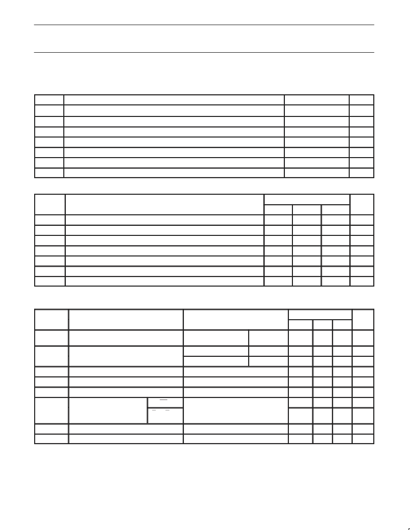
ABSOLUTE MAXIMUM RATINGS
(Operation beyond the limit set forth in this table may impair the useful life of the device.
Unless otherwise noted these limits are over the operating free-air temperature range.)
SYMBOL
PARAMETER
RATING
UNIT
V
CC
Supply voltage
–0.5 to +7.0
V
V
IN
Input voltage
–0.5 to +7.0
V
I
IN
Input current
–30 to +5
mA
V
OUT
Voltage applied to output in High output state
–0.5 to V
CC
V
I
OUT
Current applied to output in Low output state
16
mA
T
amb
Operating free-air temperature range
0 to +70
°
C
T
stg
Storage temperature range
–65 to +150
°
C
RECOMMENDED OPERATING CONDITIONS
SYMBOL
PARAMETER
LIMITS
UNIT
MIN
NOM
MAX
V
CC
Supply voltage
4.5
5.0
5.5
V
V
IH
High-level input voltage
2.0
V
V
IL
Low-level input voltage
0.8
V
I
Ik
Input clamp current
–18
mA
I
OH
High-level output current
–0.4
mA
I
OL
Low-level output current
8
mA
T
amb
Operating free-air temperature range
0
+70
°
C
DC ELECTRICAL CHARACTERISTICS
(Over recommended operating free-air temperature range unless otherwise noted.)
SYMBOL
PARAMETER
TEST CONDITIONS
1
LIMITS
UNIT
MIN
TYP
2
MAX
V
OH
High-level output voltage
V
CC
=
±
10%,
V
IL
= MAX, V
IH
= MIN
I
OH
= –0.4mA
V
CC
– 2
V
V
OL
Low level output voltage
Low-level output voltage
V
CC
= MIN, V
IL
= MAX,
I
OL
= 4mA
0.25
0.40
V
V
IH
= MIN
I
OL
= 8mA
0.35
0.50
V
V
IK
Input clamp voltage
V
CC
= MIN, I
I
= I
IK
–0.73
–1.5
V
I
I
Input current at maximum input voltage
V
CC
= MAX, V
I
= 7.0V
0.1
mA
I
IH
High-level input current
V
CC
= MAX, V
I
= 2.7V
20
μ
A
CPn
–0.1
mA
I
IL
Low-level input current
SDn, RDn,
Jn, Kn
V
CC
= MAX, V
I
= 0.4V
–0.2
mA
I
O
Output current
3
V
CC
= MAX, V
O
= 2.25V
–30
–112
mA
I
CC
Supply current (total)
V
CC
= MAX
2.5
4.5
mA
NOTES:
1. For conditions shown as MIN or MAX, use the appropriate value specified under recommended operating conditions for the applicable type.
2. All typical values are at V
= 5V, T
= 25
°
C.
3. The output conditions have been chosen to produce a current that closely approximates one half of the true short–circuit output current, I
OS
.
相关PDF资料 |
PDF描述 |
|---|---|
| 74ALS112AD | Dual J-K negative edge-triggered flip-flop |
| 74ALS112AN | Dual J-K negative edge-triggered flip-flop |
| 74ALS11AD | Triple 3-Input AND gate |
| 74ALS11A | Triple 3-Input AND gate(三3输入与门) |
| 74ALS11AN | Triple 3-Input AND gate |
相关代理商/技术参数 |
参数描述 |
|---|---|
| 74ALS112AD | 制造商:PHILIPS 制造商全称:NXP Semiconductors 功能描述:Dual J-K negative edge-triggered flip-flop |
| 74ALS112AN | 制造商:PHILIPS 制造商全称:NXP Semiconductors 功能描述:Dual J-K negative edge-triggered flip-flop |
| 74ALS11A | 制造商:PHILIPS 制造商全称:NXP Semiconductors 功能描述:Triple 3-Input AND gate |
| 74ALS11AD | 制造商:PHILIPS 制造商全称:NXP Semiconductors 功能描述:Triple 3-Input AND gate |
| 74ALS11AN | 制造商:PHILIPS 制造商全称:NXP Semiconductors 功能描述:Triple 3-Input AND gate |
发布紧急采购,3分钟左右您将得到回复。