- 您现在的位置:买卖IC网 > PDF目录360410 > 74ALS164D (NXP SEMICONDUCTORS) 8-bit serial-in parallel-out shift register PDF资料下载
参数资料
| 型号: | 74ALS164D |
| 厂商: | NXP SEMICONDUCTORS |
| 元件分类: | 通用总线功能 |
| 英文描述: | 8-bit serial-in parallel-out shift register |
| 中文描述: | ALS SERIES, 8-BIT RIGHT SERIAL IN PARALLEL OUT SHIFT REGISTER, TRUE OUTPUT, PDSO14 |
| 封装: | PLASTIC, SOT-108-1, SO-14 |
| 文件页数: | 2/9页 |
| 文件大小: | 103K |
| 代理商: | 74ALS164D |
Philips Semiconductors
Product specification
74ALS164
8-bit serial-in parallel-out shift register
2
1991 Feb 08
853–1510 01670
FEATURES
Gated serial data inputs
Typical shift frequency of 75MHz
Asynchronous master reset
Buffered clock and data inputs
Fully synchronous data transfer
DESCRIPTION
The 74ALS164 is an 8-bit edge-triggered shift register with serial
data entry and an output from each of the eight stages. Data is
entered serially through one of two inputs (Dsa, Dsb); either input
can be used as an active-high enable for data entry through the
other input. Both inputs must be connected together or an unused
input must be tied High.
Data shifts one place to the right on each Low-to-high transition of
the clock (CP) input, and enters into Q0 the logical AND of the two
data inputs (Dsa, Dsb) that existed one setup time before the rising
edge. A Low level on the Master reset (MR) input overrides all other
inputs and clears the register asynchronously, forcing all outputs
Low.
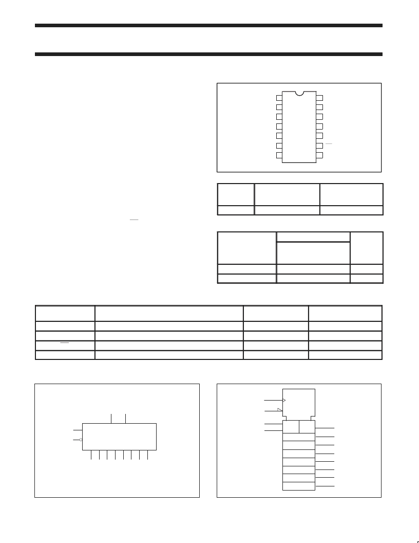
PIN CONFIGURATION
14
13
12
11
10
9
8
7
6
5
4
3
2
1
SF00717
Dsa
Dsb
Q0
Q1
Q2
Q3
GND
V
CC
Q7
Q6
Q5
Q4
MR
CP
TYPE
TYPICAL
f
MAX
TYPICAL
SUPPLY CURRENT
(TOTAL)
74ALS164
75MHz
10mA
ORDERING INFORMATION
ORDER CODE
DESCRIPTION
COMMERCIAL RANGE
V
CC
= 5V
±
10%,
T
amb
= 0
°
C to +70
°
C
DRAWING
NUMBER
14-pin plastic DIP
74ALS164N
SOT27-1
14-pin plastic SO
74ALS164D
SOT108-1
INPUT AND OUTPUT LOADING AND FAN-OUT TABLE
PINS
DESCRIPTION
74ALS (U.L.)
HIGH/LOW
LOAD VALUE
HIGH/LOW
Dsa, Dsb
Data inputs
1.0/1.0
20
μ
A/0.1mA
20
μ
A/0.1mA
20
μ
A/0.1mA
CP
Clock Pulse input (active rising edge)
1.0/1.0
MR
Master Reset input (active-Low)
1.0/1.0
Q0 – Q7
One (1.0) ALS unit load is defined as: 20
μ
A in the High state and 0.1mA in the Low state.
Data outputs
20/80
0.4mA/8mA
NOTE:
LOGIC SYMBOL
Dsa
Dsb
Q0
1
2
V
= Pin 14
GND = Pin 7
Q1 Q3 Q4 Q0 Q1 Q3 Q4
CP
MR
8
9
SF00713
3
4
5
6 10
11
12 13
IEC/IEEE SYMBOL
1
2
SRG8
&
R
C1/
→
8
9
1D
SF00714
3
4
5
6
10
11
12
13
相关PDF资料 |
PDF描述 |
|---|---|
| 74ALS164N | 8-bit serial-in parallel-out shift register |
| 74ALS174 | Hex D flip-flop |
| 74ALS174D | Hex D flip-flop |
| 74ALS174N | Hex D flip-flop |
| 74ALS175 | Quad D flip-flop |
相关代理商/技术参数 |
参数描述 |
|---|---|
| 74ALS164N | 制造商:NXP Semiconductors 功能描述: |
| 74ALS169BN TI91 | 制造商:TI 功能描述:74ALS169N |
| 74ALS169BNTI91 | 制造商:TI 功能描述:74ALS169N |
| 74ALS174 | 制造商:PHILIPS 制造商全称:NXP Semiconductors 功能描述:Hex D flip-flop |
| 74ALS174D | 制造商:PHILIPS 制造商全称:NXP Semiconductors 功能描述:Hex D flip-flop |
发布紧急采购,3分钟左右您将得到回复。