- 您现在的位置:买卖IC网 > PDF目录360417 > 74ALVCH16646 (NXP Semiconductors N.V.) Quadruple Positive-NAND Gates With Schmitt-Trigger Inputs 14-TSSOP -40 to 85 PDF资料下载
参数资料
| 型号: | 74ALVCH16646 |
| 厂商: | NXP Semiconductors N.V. |
| 英文描述: | Quadruple Positive-NAND Gates With Schmitt-Trigger Inputs 14-TSSOP -40 to 85 |
| 中文描述: | 16位总线收发器/寄存器三态 |
| 文件页数: | 2/12页 |
| 文件大小: | 92K |
| 代理商: | 74ALVCH16646 |
Philips Semiconductors
Product specification
74ALVCH16646
16-bit bus transceiver/register (3-State)
2
1998 Sep 03
853-2116 19959
FEATURES
Complies with JEDEC standard no. 8-1A
CMOS low power consumption
MULTIBYTE
TM
flow-through pin-out architecture
Low inductance, multiple V
CC
and ground pins for minimum noise
and ground bounce
Direct interface with TTL levels
Current drive
±
24 mA at 3.0 V
Output drive capability 50
transmission lines @ 85
°
C
All inputs have bushold circuitry
DESCRIPTION
The 74ALVCH16646 consists of 16 non-inverting bus transceiver
circuits with 3-State outputs, D-type flip-flops and control circuitry
arranged for multiplexed transmission of data directly from the
internal registers. Data on the ‘A’ or ‘B’ bus will be clocked in the
internal registers, as the appropriate clock (CP
AB
or CP
BA
) goes to a
HIGH logic level. Output enable (OE) and direction (DIR) inputs are
provided to control the transceiver function. In the transceiver mode,
data present at the high-impedance port may be stored in either the
‘A’ or ‘B’ register, or in both. The select source inputs (S
AB
and S
BA
)
can multiplex stored and real-time (transparent mode) data. The
direction (DIR) input determines which bus will receive data when
OE is active (LOW). In the isolation mode (OE = HIGH), ‘A’ data
may be stored in the ‘B’ register and/or ‘B’ data may be stored in the
‘A’ register.
When an output function is disabled, the input function is still
enabled and may be used to store and transmit data. Only one of
the two buses, ‘A’ or ‘B’ may be driven at a time.
To ensure the high impedance state during power up or power
down, OE should be tied to V
CC
through a pullup resistor; the
minimum value of the resistor is determined by the
current-sinking/current-sourcing capability of the driver.
Active bus-hold circuitry is provided to hold unused or floating data
inputs at a valid logic level.
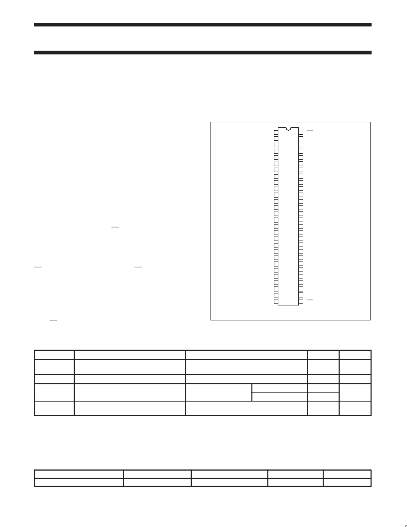
PIN CONFIGURATION
1
2
3
4
5
6
7
8
9
10
11
12
13
14
15
16
17
18
19
20
21
22
23
24
25
26
27
28
37
36
38
39
40
41
42
43
44
45
46
47
48
49
50
51
52
53
54
55
56
1DIR
1CP
AB
1S
AB
GND
1A0
1A1
V
CC
1A2
1A3
1A4
GND
1A5
1A6
1A7
2A0
2A1
2A2
GND
2A3
2A4
2A5
V
CC
2A6
2A7
GND
2S
AB
2CP
AB
2DIR
2B4
2B5
2B3
GND
2B2
2B1
2B0
1B7
1B6
1B5
GND
1B4
1B3
1B2
V
CC
1B1
1B0
GND
1S
BA
1CP
BA
1OE
33
32
34
35
2B7
GND
2B6
V
CC
29
30
31
2OE
2CP
BA
2S
BA
SY00011
QUICK REFERENCE DATA
GND = 0V; T
amb
= 25
°
C; t
r
= t
f
≤
2.5ns
SYMBOL
PARAMETER
CONDITIONS
TYPICAL
UNIT
t
PHL
/t
PLH
Propagation delay
nAx to nBx
V
CC
= 2.5V, C
L
= 30pF
V
CC
= 3.3V, C
L
= 50pF
2.6
2.7
ns
C
I
Input capacitance
3.0
pF
C
PD
Power dissipation capacitance per channel
V = GND to V
CC1
Outputs enabled
36
pF
Outputs disabled
4
F
max
Maximum clock frequency
V
CC
= 2.5V, C
L
= 30pF
V
CC
= 3.3V, C
L
= 50pF
300
320
MHz
NOTES:
1. C
PD
is used to determine the dynamic power dissipation (P
D
in
μ
W):
P
D
= C
PD
×
V
CC2
×
f
i
+ (C
L
×
V
CC2
×
f
o
) where:
f
i
= input frequency in MHz; C
L
= output load capacity in pF;
f
o
= output frequency in MHz; V
CC
= supply voltage in V;
(C
L
×
V
CC2
×
f
o
) = sum of outputs.
ORDERING INFORMATION
PACKAGES
56-Pin Plastic TSSOP Type II
TEMPERATURE RANGE
–40
°
C to +85
°
C
OUTSIDE NORTH AMERICA
74ALVCH16646 DGG
NORTH AMERICA
ACH16646 DGG
DWG NUMBER
SOT364-1
相关PDF资料 |
PDF描述 |
|---|---|
| 74ALVCH16652 | 16-bit transceiver/register with dual enable; 3-state |
| 74ALVCH16821 | Quadruple Positive-NAND Gates With Schmitt-Trigger Inputs 14-TSSOP -40 to 85 |
| 74ALVCH16823 | Automotive Catalog Quadruple Positive-NAND Gates With Schmitt-Trigger Inputs 14-SOIC -40 to 125 |
| 74ALVCH16825 | Automotive Catalog Quadruple Positive-NAND Gates With Schmitt-Trigger Inputs 14-TSSOP -40 to 125 |
| 74ALVCH16827 | 20-bit buffer/line driver, non-inverting 3-State |
相关代理商/技术参数 |
参数描述 |
|---|---|
| 74ALVCH16646APA | 制造商:Rochester Electronics LLC 功能描述:- Bulk |
| 74ALVCH16646DG | 功能描述:总线收发器 18BIT UNIV. BUS TRANXCVR 3-ST RoHS:否 制造商:Fairchild Semiconductor 逻辑类型:CMOS 逻辑系列:74VCX 每芯片的通道数量:16 输入电平:CMOS 输出电平:CMOS 输出类型:3-State 高电平输出电流:- 24 mA 低电平输出电流:24 mA 传播延迟时间:6.2 ns 电源电压-最大:2.7 V, 3.6 V 电源电压-最小:1.65 V, 2.3 V 最大工作温度:+ 85 C 封装 / 箱体:TSSOP-48 封装:Reel |
| 74ALVCH16646DGG | 制造商:PHILIPS 制造商全称:NXP Semiconductors 功能描述:16-bit bus transceiver/register 3-State |
| 74ALVCH16646DGG,11 | 功能描述:总线收发器 18BIT UNIV. BUS RoHS:否 制造商:Fairchild Semiconductor 逻辑类型:CMOS 逻辑系列:74VCX 每芯片的通道数量:16 输入电平:CMOS 输出电平:CMOS 输出类型:3-State 高电平输出电流:- 24 mA 低电平输出电流:24 mA 传播延迟时间:6.2 ns 电源电压-最大:2.7 V, 3.6 V 电源电压-最小:1.65 V, 2.3 V 最大工作温度:+ 85 C 封装 / 箱体:TSSOP-48 封装:Reel |
| 74ALVCH16646DGG,112 | 制造商:NXP Semiconductors 功能描述: |
发布紧急采购,3分钟左右您将得到回复。