- 您现在的位置:买卖IC网 > PDF目录360417 > 74ALVCH16827 (NXP Semiconductors N.V.) 20-bit buffer/line driver, non-inverting 3-State PDF资料下载
参数资料
| 型号: | 74ALVCH16827 |
| 厂商: | NXP Semiconductors N.V. |
| 英文描述: | 20-bit buffer/line driver, non-inverting 3-State |
| 中文描述: | 20位缓冲器/线路驱动器,非反相三态 |
| 文件页数: | 2/10页 |
| 文件大小: | 72K |
| 代理商: | 74ALVCH16827 |
Philips Semiconductors
Product specification
74ALVCH16827
20-bit buffer/line driver, non-inverting (3-State)
2
1998 Jul 27
853-2096 19785
FEATURES
Wide supply voltage range of 1.2V to 3.6V
Complies with JEDEC standard no. 8-1A
Wide supply voltage range of 1.2V to 3.6V
CMOS low power consumption
Direct interface with TTL levels
Universal bus transceiver with D-type latches and D-type flip-flops
capable of operating in transparent, latched, clocked or
clocked-enabled mode.
MULTIBYTE
TM
flow-through standard pin-out architecture
Low inductance multiple V
CC
and GND pins for minimum noise
and ground bounce
Current drive
±
24 mA at 3.0 V
All inputs have bus hold circuitry
Output drive capability 50
transmission lines @ 85
°
C
3-State non-inverting outputs for bus oriented applications
DESCRIPTION
The 74ALVCH16827 is a 20-bit non-inverting buffer/driver with
3-State outputs for bus oriented applications.
The 74ALVCH16827 consists of two 10-bit sections with separate
output enable signals. For either 10-bit buffer section, the two output
enable (1OE1 and 1OE2 or 2OE1 and 2OE2) inputs must both be
active. If either output enable input is high, the outputs of that 10-bit
buffer section are in high impedance state.
The 74ALVCH16827 has active bus hold circuitry which is provided
to hold unused or floating data inputs at a valid logic level. This
feature eliminates the need for external pull-up or pull-down
resistors.
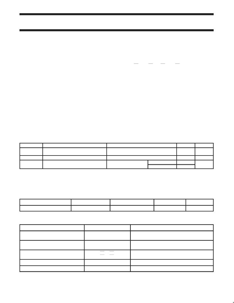
QUICK REFERENCE DATA
GND = 0V; T
amb
= 25
°
C; t
r
= t
f
= 2.5ns
SYMBOL
Propagation delay
CP to Qn
C
I
Input capacitance
PARAMETER
CONDITIONS
TYPICAL
2.0
2.0
5
20
3
UNIT
t
PHL
/t
PLH
V
CC
= 2.5V, C
L
= 30pF
V
CC
= 3.3V, C
L
= 50pF
ns
pF
PD
C
Power dissipation capacitance per latch
Power dissi ation ca acitance er latch
I
V
= GND to V
CC1
Output enabled
Output disabled
pF
NOTES:
1.
C
PD
is used to determine the dynamic power dissipation (P
D
in W):
P
D
= C
PD
×
V
CC2
×
f
i
+ (C
L
×
V
CC2
×
f
o
) where:
f
i
= input frequency in MHz; C
L
= output load capacity in pF;
f
o
= output frequency in MHz; V
CC
= supply voltage in V;
(C
L
×
V
CC2
×
f
o
) = sum of outputs.
ORDERING INFORMATION
PACKAGES
TEMPERATURE RANGE
OUTSIDE NORTH AMERICA
NORTH AMERICA
DWG NUMBER
56-Pin Plastic TSSOP Type II
–40
°
C to +85
°
C
74ALVCH16827 DGG
ACH16827 DGG
SOT364-1
PIN DESCRIPTION
PIN NUMBER
SYMBOL
FUNCTION
55, 54, 52, 51, 49, 48, 47, 45, 44, 43,
42, 41, 40, 38, 37, 36, 34, 33, 31, 30
1A0 - 1A9
2A0 - 2A9
Data inputs
2, 3, 5, 6, 8, 9, 10, 12, 13, 14,
15, 16, 17, 19, 20, 21, 23, 24, 26, 27
1Y0 - 1Y9
2Y0 - 2Y9
Data outputs
1, 56,
28, 29
1OE0, 1OE1
2OE0, 2OE1
Output enable inputs (active-Low)
4, 11, 18, 25, 32, 39, 46, 53
GND
Ground (0V)
7, 22, 35, 50
V
CC
Positive supply voltage
相关PDF资料 |
PDF描述 |
|---|---|
| 74ALVCH16841DL | 20-bit bus interface D-type latch (3-State) |
| 74ALVCH16841 | 20-bit bus interface D-type latch 3-State |
| 74ALVCH16843 | 3-Line To 8-Line Decoders/Demultiplexers 16-SSOP -40 to 85 |
| 74ALVCH16952 | 16-bit registered transceiver 3-State |
| 74ALVCH32501 | 3-Line To 8-Line Decoders/Demultiplexers 16-PDIP -40 to 85 |
相关代理商/技术参数 |
参数描述 |
|---|---|
| 74ALVCH16827APV | 制造商:Rochester Electronics LLC 功能描述:- Bulk 制造商:Integrated Device Technology Inc 功能描述: |
| 74ALVCH16827DG | 功能描述:缓冲器和线路驱动器 21 BIT BUF/DVR 3-S RoHS:否 制造商:Micrel 输入线路数量:1 输出线路数量:2 极性:Non-Inverting 电源电压-最大:+/- 5.5 V 电源电压-最小:+/- 2.37 V 最大工作温度:+ 85 C 安装风格:SMD/SMT 封装 / 箱体:MSOP-8 封装:Reel |
| 74ALVCH16827DGG | 制造商:PHILIPS 制造商全称:NXP Semiconductors 功能描述:20-bit buffer/line driver, non-inverting 3-State |
| 74ALVCH16827DGG,11 | 功能描述:缓冲器和线路驱动器 22 BIT BUF/DVR 3-S RoHS:否 制造商:Micrel 输入线路数量:1 输出线路数量:2 极性:Non-Inverting 电源电压-最大:+/- 5.5 V 电源电压-最小:+/- 2.37 V 最大工作温度:+ 85 C 安装风格:SMD/SMT 封装 / 箱体:MSOP-8 封装:Reel |
| 74ALVCH16827DGG,112 | 制造商:NXP Semiconductors 功能描述: |
发布紧急采购,3分钟左右您将得到回复。