- 您现在的位置:买卖IC网 > PDF目录360417 > 74ALVCH16841 (NXP Semiconductors N.V.) 20-bit bus interface D-type latch 3-State PDF资料下载
参数资料
| 型号: | 74ALVCH16841 |
| 厂商: | NXP Semiconductors N.V. |
| 英文描述: | 20-bit bus interface D-type latch 3-State |
| 中文描述: | 20位总线接口,D型锁存器三态 |
| 文件页数: | 2/10页 |
| 文件大小: | 77K |
| 代理商: | 74ALVCH16841 |
Philips Semiconductors
Product specification
74ALVCH16841
20-bit bus interface D-type latch (3-State)
2
1998 Jul 27
853-2093 19785
FEATURES
Wide supply voltage range of 1.2V to 3.6V
Complies with JEDEC standard no. 8-1A
Wide supply voltage range of 1.2V to 3.6V
CMOS low power consumption
Direct interface with TTL levels
MULTIBYTE
TM
flow-through standard pin-out architecture
Low inductance multiple V
CC
and GND pins for minimum noise
and ground bounce
Current drive
±
24 mA at 3.0 V
All inputs have bus hold circuitry
Output drive capability 50
transmission lines @ 85
°
C
3-State non-inverting outputs for bus oriented applications
DESCRIPTION
The 74ALVCH16841 has two 10-bit D-type latch featuring separate
D-type inputs for each latch and 3-State outputs for bus oriented
applications. The two sections of each register are controlled
independently by the latch enable (nLE) and output enable (nOE)
control gates.
When nOE is LOW, the data in the registers appears at the outputs.
When nOE is High the outputs are in High-impedance OFF state.
Operation of the nOE input does not affect the state of the flip-flops.
The 74ALVCH16841 has active bus hold circuitry which is provided
to hold unused or floating data inputs at a valid logic level. This
feature eliminates the need for external pull-up or pull-down
resistors.
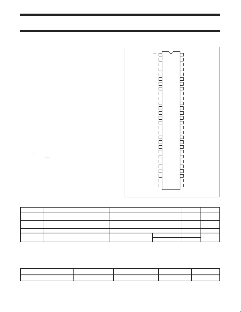
PIN CONFIGURATION
1
2
3
4
5
6
7
8
9
10
11
12
13
14
15
16
17
18
19
20
21
22
23
24
48
47
46
45
44
43
42
41
40
39
38
37
36
35
34
33
32
31
30
29
1OE
1Q0
1Q1
GND
1Q2
1Q3
1Q4
1Q5
GND
1Q6
1Q7
1Q8
2Q2
1Q9
V
CC
2Q6
2Q3
V
CC
2Q1
2Q4
2Q8
2OE
2Q7
1LE
1D0
1D1
GND
1D2
1D3
1D4
1D5
2D0
1D6
1D7
2D1
2D2
GND
2D4
V
CC
2D6
2D5
V
CC
2D3
GND
2D8
2LE
2D7
SA00076
2Q0
GND
2Q5
28
27
26
25
49
50
51
52
53
54
55
56
2D9
1D9
1D8
GND
2Q9
GND
QUICK REFERENCE DATA
GND = 0V; T
amb
= 25
°
C; t
r
= t
f
≤
2.5ns
SYMBOL
Propagation delay
nD
n
to nQ
n
Propagation delay
nLE to nQ
n
C
I
Input capacitance
PARAMETER
CONDITIONS
TYPICAL
2.5
2.4
2.5
2.4
5.0
19
3
UNIT
t
PHL
/t
PLH
V
CC
= 2.5V, C
L
= 30pF
V
CC
= 3.3V, C
L
= 50pF
V
CC
= 2.5V, C
L
= 30pF
V
CC
= 3.3V, C
L
= 50pF
ns
t
PHL
/t
PLH
ns
pF
C
PD
Power dissipation capacitance per buffer
Power dissi ation ca acitance er buffer
V
I
= GND to V
CC1
Outputs enabled
Outputs disabled
pF
NOTES:
1. C
PD
is used to determine the dynamic power dissipation (P
D
in
μ
W):
P
D
= C
×
V
CC2
×
f
+ (C
×
V
CC2
×
f
) where: f
= input frequency in MHz; C
= output load capacitance in pF;
f
o
= output frequency in MHz; V
CC
= supply voltage in V; (C
L
×
V
CC2
×
f
o
) = sum of outputs.
ORDERING INFORMATION
PACKAGES
TEMPERATURE RANGE
OUTSIDE NORTH AMERICA
NORTH AMERICA
DWG NUMBER
56-Pin Plastic TSSOP Type II
–40
°
C to +85
°
C
74ALVCH16841 DGG
ACH16841 DGG
SOT364-1
相关PDF资料 |
PDF描述 |
|---|---|
| 74ALVCH16843 | 3-Line To 8-Line Decoders/Demultiplexers 16-SSOP -40 to 85 |
| 74ALVCH16952 | 16-bit registered transceiver 3-State |
| 74ALVCH32501 | 3-Line To 8-Line Decoders/Demultiplexers 16-PDIP -40 to 85 |
| 74ALVCH32501EC | 36-bit universal bus transceiver with direction pin; 5 V tolerant; 3-state |
| 74ALVCHS162830 | 18-bit to 36-bit address driver with bus hold (3-State) |
相关代理商/技术参数 |
参数描述 |
|---|---|
| 74ALVCH16841DG | 功能描述:闭锁 20-BIT BUS INTERD LATCH 3-S RoHS:否 制造商:Micrel 电路数量:1 逻辑类型:CMOS 逻辑系列:TTL 极性:Non-Inverting 输出线路数量:9 高电平输出电流: 低电平输出电流: 传播延迟时间: 电源电压-最大:12 V 电源电压-最小:5 V 最大工作温度:+ 85 C 最小工作温度:- 40 C 封装 / 箱体:SOIC-16 封装:Reel |
| 74ALVCH16841DGG | 制造商:PHILIPS 制造商全称:NXP Semiconductors 功能描述:20-bit bus interface D-type latch 3-State |
| 74ALVCH16841DGG,11 | 功能描述:闭锁 20-BIT BUS INTERD RoHS:否 制造商:Micrel 电路数量:1 逻辑类型:CMOS 逻辑系列:TTL 极性:Non-Inverting 输出线路数量:9 高电平输出电流: 低电平输出电流: 传播延迟时间: 电源电压-最大:12 V 电源电压-最小:5 V 最大工作温度:+ 85 C 最小工作温度:- 40 C 封装 / 箱体:SOIC-16 封装:Reel |
| 74ALVCH16841DGG,112 | 制造商:NXP Semiconductors 功能描述: |
| 74ALVCH16841DGG,118 | 制造商:NXP Semiconductors 功能描述: |
发布紧急采购,3分钟左右您将得到回复。