- 您现在的位置:买卖IC网 > PDF目录360417 > 74ALVT162240 (NXP Semiconductors N.V.) 16-bit inverting buffer/driver with 30 Ωtermination resistors (3-State)(带30 Ω终端电阻器的16位反相缓冲器/驱动器(三态)) PDF资料下载
参数资料
| 型号: | 74ALVT162240 |
| 厂商: | NXP Semiconductors N.V. |
| 英文描述: | 16-bit inverting buffer/driver with 30 Ωtermination resistors (3-State)(带30 Ω终端电阻器的16位反相缓冲器/驱动器(三态)) |
| 中文描述: | 16位反相缓冲器/ 30Ωtermination电阻(3态)(带30Ω终端电阻器的16位反相缓冲器/驱动器驱动器(三态)) |
| 文件页数: | 4/10页 |
| 文件大小: | 86K |
| 代理商: | 74ALVT162240 |
Philips Semiconductors
Product specification
74ALVT162240
2.5V/3.3V 16-bit inverting buffer/driver with
30
termination resistors (3-State)
1998 Feb 13
4
NOTES:
1. Stresses beyond those listed may cause permanent damage to the device. These are stress ratings only and functional operation of the
device at these or any other conditions beyond those indicated under “recommended operating conditions” is not implied. Exposure to
absolute-maximum-rated conditions for extended periods may affect device reliability.
2. The performance capability of a high-performance integrated circuit in conjunction with its thermal environment can create junction
temperatures which are detrimental to reliability. The maximum junction temperature of this integrated circuit should not exceed 150
°
C.
3. The input and output negative voltage ratings may be exceeded if the input and output clamp current ratings are observed.
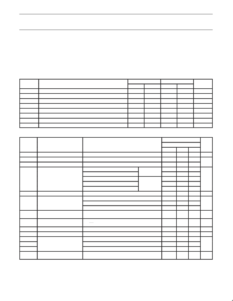
RECOMMENDED OPERATING CONDITIONS
SYMBOL
PARAMETER
2.5V RANGE LIMITS
MIN
2.3
0
1.7
3.3V RANGE LIMITS
MIN
3.0
0
2.0
UNIT
MAX
2.7
5.5
MAX
3.6
5.5
V
CC
V
I
V
IH
V
IL
I
OH
I
OL
t/
v
T
amb
DC supply voltage
Input voltage
High-level input voltage
Input voltage
High-level output current
Low-level output current
Input transition rise or fall rate; Outputs enabled
Operating free-air temperature range
V
V
V
V
0.7
–8
12
10
+85
0.8
–12
12
10
+85
mA
mA
ns/V
°
C
–40
–40
DC ELECTRICAL CHARACTERISTICS (3.3V
0.3V RANGE)
LIMITS
SYMBOL
PARAMETER
TEST CONDITIONS
Temp = -40
°
C to +85
°
C
MIN
TYP
1
–0.85
2.0
2.5
0.5
0.1
0.1
0.1
0.5
0.1
0.1
75
130
–75
–140
±
500
UNIT
MAX
–1.2
2.5
0.8
±
1
10
10
1
-5
±
100
V
IK
V
OH
V
OL
Input clamp voltage
High-level output voltage
Low–level output voltage
V
CC
= 3.0V; I
IK
= –18mA
V
CC
= 3.0V; I
OH
= –12mA
V
CC
= 3.0V; I
OL
= 12mA
V
CC
= 3.6V; V
I
= V
CC
or GND
V
CC
= 0 or 3.6V; V
I
= 5.5V
V
CC
= 3.6V; V
I
= 5.5V
V
CC
= 3.6V; V
I
= V
CC
V
CC
= 3.6V; V
I
= 0
V
CC
= 0V; V
I
or V
O
= 0 to 4.5V
V
CC
= 3.0V; V
I
= 0.8V
V
CC
= 3.0V; V
I
= 2.0V
V
I
= 0V to 3.6V; V
CC
= 3.6V
V
V
V
Control pins
Control ins
I
I
Input leakage current
μ
A
Data pins
4
I
OFF
Off current
μ
A
Bus Hold current
Data inputs
5
I
HOLD
μ
A
I
EX
Current into an output in the
High state when V
O
> V
CC
Power up/down 3-State output
current
3
3-State output High current
3-State output Low current
V
O
= 5.5V; V
CC
= 3.0V
10
125
μ
A
I
PU/PD
V
≤
1.2V; V
= 0.5V to V
CC
; V
I
= GND or V
CC
;
OE/OE = Don’t care
V
CC
= 3.6V; V
O
= 3.0V; V
I
= V
IL
or V
IH
V
CC
= 3.6V; V
O
= 0.5V; V
I
= V
IL
or V
IH
V
CC
= 3.6V; Outputs High, V
I
= GND or V
CC,
I
O
=
0
V
CC
= 3.6V; Outputs Low, V
I
= GND or V
CC,
I
O
=
0
V
CC
= 3.6V; Outputs Disabled; V
I
= GND or V
CC,
I
O
=
0
5
V
= 3V to 3.6V; One input at V
CC
–0.6V,
Other inputs at V
CC
or GND
1
±
100
μ
A
I
OZH
I
OZL
I
CCH
I
CCL
I
CCZ
0.5
0.5
0.05
3.6
0.06
5
–5
0.1
5.5
0.1
μ
A
μ
A
Quiescent supply current
mA
I
CC
Additional supply current per
input pin
2
0.1
0.4
mA
NOTES:
1. All typical values are at V
= 3.3V and T
= 25
°
C.
2. This is the increase in supply current for each input at the specified voltage level other than V
or GND
3. This parameter is valid for any V
between 0V and 1.2V with a transition time of up to 10msec. From V
CC
= 1.2V to V
CC
= 3.3V
±
0.3V a
transition time of 100
μ
sec is permitted. This parameter is valid for T
amb
= 25
°
C only.
4. Unused pins at V
CC
or GND.
5. I
CCZ
is measured with outputs pulled up to V
CC
or pulled down to ground.
相关PDF资料 |
PDF描述 |
|---|---|
| 74ALVT162241 | 2.5V/3.3V 16-bit buffer/driver with 30 Ωtermination resistors (3-State)(带30 Ω终端电阻器的2.5V/3.3V 16位缓冲器/驱动器(三态)) |
| 74ALVT162244 | 2.5V/3.3V 16-bit buffer/driver with 30 Ωtermination resistors (3-State)(带30 Ω终端电阻器的2.5V/3.3V 16位缓冲器/驱动器(三态)) |
| 74ALVT162344DL | 2.5V/3.3V 1-to-4 address driver with 30ohm termination resistors 3-State |
| 74ALVT162344 | 2.5V/3.3V 1-to-4 address driver with 30Ω termination resistors (3-State)(带30 Ω终端电阻器的2.5V/3.3V 1至4地址驱动器 (三态)) |
| 74ALVT162344DGG | 2.5V/3.3V 1-to-4 address driver with 30ohm termination resistors 3-State |
相关代理商/技术参数 |
参数描述 |
|---|---|
| 74ALVT162240DG | 功能描述:缓冲器和线路驱动器 2.5/3.3V 16-BIT BUFFER INV 3-S RoHS:否 制造商:Micrel 输入线路数量:1 输出线路数量:2 极性:Non-Inverting 电源电压-最大:+/- 5.5 V 电源电压-最小:+/- 2.37 V 最大工作温度:+ 85 C 安装风格:SMD/SMT 封装 / 箱体:MSOP-8 封装:Reel |
| 74ALVT162240DGG | 制造商:PHILIPS 制造商全称:NXP Semiconductors 功能描述:16-bit inverting buffer/driver with 30ohm termination resistors (3-State) |
| 74ALVT162240DGG,11 | 功能描述:缓冲器和线路驱动器 IC BUFF DVR TRI-ST 16BIT RoHS:否 制造商:Micrel 输入线路数量:1 输出线路数量:2 极性:Non-Inverting 电源电压-最大:+/- 5.5 V 电源电压-最小:+/- 2.37 V 最大工作温度:+ 85 C 安装风格:SMD/SMT 封装 / 箱体:MSOP-8 封装:Reel |
| 74ALVT162240DGG,112 | 制造商:NXP Semiconductors 功能描述: |
| 74ALVT162240DGG,118 | 制造商:NXP Semiconductors 功能描述: |
发布紧急采购,3分钟左右您将得到回复。