- 您现在的位置:买卖IC网 > PDF目录360419 > 74AVCM162834 (NXP Semiconductors N.V.) 18-bit registered driver with inverted register enable with 15Ω termination resistors (3-State)(带15Ω终端电阻的具有反相寄存使能的18位寄存驱动器(三态)) PDF资料下载
参数资料
| 型号: | 74AVCM162834 |
| 厂商: | NXP Semiconductors N.V. |
| 英文描述: | 18-bit registered driver with inverted register enable with 15Ω termination resistors (3-State)(带15Ω终端电阻的具有反相寄存使能的18位寄存驱动器(三态)) |
| 中文描述: | 18位与倒登记册登记的司机能够与15Ω终端电阻(3态)(带15Ω终端电阻的具有反相寄存使能的18位寄存驱动器(三态)) |
| 文件页数: | 7/10页 |
| 文件大小: | 89K |
| 代理商: | 74AVCM162834 |
Philips Semiconductors
Product specification
74AVCM162834
18-bit registered driver with inverted register enable with
15
termination resistors (3-State)
1999 Sep 14
7
AC WAVEFORMS FOR V
CC
= 3.0 V TO 3.6 V RANGE
V
M
= 0.5 V
V
X
= V
OL
+ 0.300 V
V
Y
= V
OH
– 0.300 V
V
OL
and V
OH
are the typical output voltage drop that occur with the
output load.
V
I
= V
CC
AC WAVEFORMS FOR V
CC
= 2.3 V TO 2.7 V AND
V
CC
< 2.3 V RANGE
V
M
= 0.5 V
CC
V
X
= V
OL
+ 0.15 V
V
Y
= V
– 0.15 V
V
and V
OH
are the typical output voltage drop that occur with the
output load.
V
I
= V
CC
A
INPUT
t
PHL
t
PLH
V
OL
V
I
GND
V
OH
Y
OUTPUT
SH00132
V
M
V
M
NOTE: V
M
= 0.5V
CC
at V
CC
= 2.3 to 2.7 V
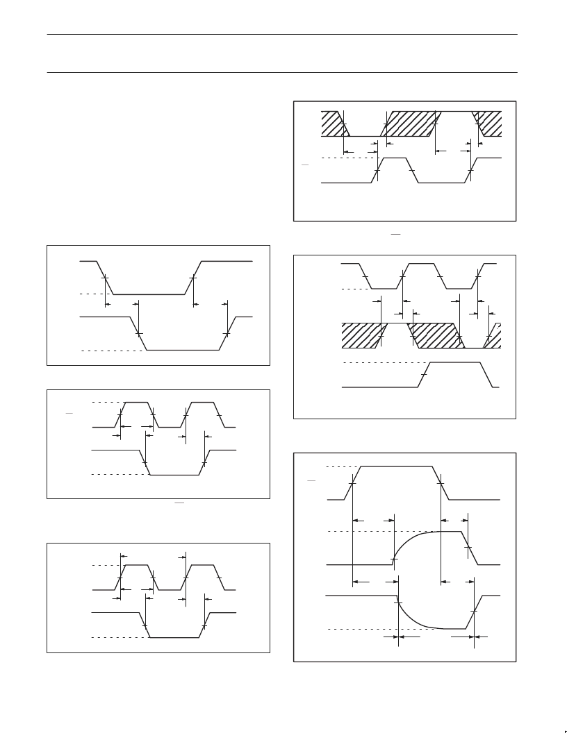
Waveform 1. Input (An) to output (Yn) propagation delay
LE INPUT
Yn OUTPUT
V
I
GND
V
OH
V
OL
t
PHL
t
PLH
t
W
V
M
V
M
V
M
SH00165
NOTE: V
M
= 0.5 V
CC
at V
CC
= 2.3 to 2.7 V
Waveform 2. Latch enable input (LE) pulse width, the latch
enable input to output (Yn) propagation delays.
CP INPUT
Yn OUTPUT
V
I
GND
V
OH
V
OL
t
PHL
t
PLH
t
W
1/f
MAX
SH00135
V
M
V
M
V
M
NOTE: V
M
= 0.5V
CC
at V
CC
= 2.3 to 2.7 V
Waveform 3. The clock (CP) to Yn propagation delays, the
clock pulse width and the maximum clock frequency.
ééé
ééé
ééééééééé
ééééééééé
ééééééééé
An
INPUT
LE
INPUT
t
SU
NOTE:
The shaded areas indicate when the input is permitted to change
for predictable output performance.
V
M
= 0.5V
CC
at V
CC
= 2.3 to 2.7 V
t
SU
V
GND
V
I
GND
V
M
V
M
SH00166
Waveform 4. Data set-up and hold times for the An input to the
LE input
V
I
GND
éééé
éééé
éééé
ééééééé
ééééééé
ééééééé
An INPUT
V
I
GND
V
OH
Yn OUTPUT
V
OL
CP INPUT
t
su
t
su
NOTE:
The shaded areas indicate when the input is permitted to change
for predictable output performance.
V
M
= 0.5V
CC
at V
CC
= 2.3 to 2.7 V
SH00136
V
M
V
M
Waveform 5. Data set-up and hold times for the An input to the
clock CP input
t
PLZ
t
PZL
V
I
nOE INPUT
GND
V
CC
OUTPUT
LOW-to-OFF
OFF-to-LOW
V
OL
V
OH
OUTPUT
HIGH-to-OFF
OFF-to-HIGH
GND
outputs
enabled
outputs
enabled
outputs
disabled
t
PHZ
V
M
V
M
V
M
t
PZH
V
X
V
Y
SH00137
NOTE: V
M
= 0.5V
CC
at V
CC
= 2.3 to 2.7 V
Waveform 6. 3-State enable and disable times
相关PDF资料 |
PDF描述 |
|---|---|
| 74AVCM162835 | 18-bit registered driver with 15Ω termination resistors (3-State)(带15Ω终端电阻的18位寄存驱动器(三态)) |
| 74AVCM162836 | 20-bit registered driver with inverted register enable and 15 ohm termination resistors 3-State |
| 74AVCM62836 | 20-bit registered driver with inverted register enable with 15Ω termination resistors (3-State)(带15Ω终端电阻的具有反相寄存使能的20位寄存驱动器(三态)) |
| 74B2529 | |
| 74B304 | |
相关代理商/技术参数 |
参数描述 |
|---|---|
| 74AVCM162834DG | 功能描述:转换 - 电压电平 18-BOT REG DRIVER W/15 W TERM RoHS:否 制造商:Micrel 类型:CML/LVDS/LVPECL to LVCMOS/LVTTL 传播延迟时间:1.9 ns 电源电流:14 mA 电源电压-最大:3.6 V 电源电压-最小:3 V 最大工作温度:+ 85 C 安装风格:SMD/SMT 封装 / 箱体:MLF-8 |
| 74AVCM162834DGG | 制造商:PHILIPS 制造商全称:NXP Semiconductors 功能描述:18-bit registered driver with inverted register enable and 15 ohm termination resistors 3-State |
| 74AVCM162834DGG,11 | 功能描述:数字总线开关 IC 18-BOT REG DRIVER RoHS:否 制造商:Texas Instruments 开关数量:24 传播延迟时间:0.25 ns 最大工作温度:+ 85 C 最小工作温度:- 40 C 封装 / 箱体:TSSOP-56 封装:Reel |
| 74AVCM162834DGG,112 | 制造商:NXP Semiconductors 功能描述: |
| 74AVCM162834DGG,118 | 制造商:NXP Semiconductors 功能描述: |
发布紧急采购,3分钟左右您将得到回复。