- 您现在的位置:买卖IC网 > PDF目录2058 > 74CB3T3306DCTRG4 (Texas Instruments)IC 3.3V DUAL FET BUS SWITCH SM8 PDF资料下载
参数资料
| 型号: | 74CB3T3306DCTRG4 |
| 厂商: | Texas Instruments |
| 文件页数: | 10/15页 |
| 文件大小: | 0K |
| 描述: | IC 3.3V DUAL FET BUS SWITCH SM8 |
| 标准包装: | 3,000 |
| 系列: | 74CB |
| 类型: | FET 总线开关 |
| 电路: | 1 x 1:1 |
| 独立电路: | 2 |
| 输出电流高,低: | 32mA,64mA |
| 电压电源: | 单电源 |
| 电源电压: | 2.3 V ~ 3.6 V |
| 工作温度: | -40°C ~ 85°C |
| 安装类型: | 表面贴装 |
| 封装/外壳: | 7-LSSOP(0.11"?,2.80mm 宽) |
| 供应商设备封装: | SM8 |
| 包装: | 带卷 (TR) |
SCDS119B – JANUARY 2003 – REVISED AUGUST 2012
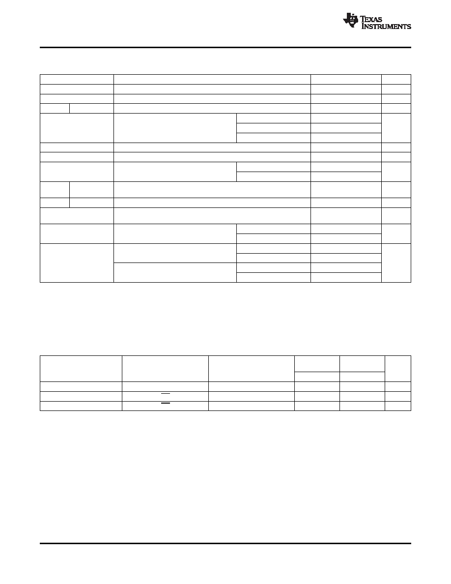
Electrical Characteristics
(1)
over recommended operating free-air temperature range (unless otherwise noted)
PARAMETER
TEST CONDITIONS
MIN
TYP(2)
MAX
UNIT
VIK
VCC = 3 V, II = –18 mA
–1.2
V
VOH
IIN
Control inputs
VCC = 3.6 V, VIN = 3.6 V to 5.5 V or GND
±10
μA
VI = VCC – 0.7 V to 5.5 V
±20
VCC = 3.6 V, Switch ON,
II
VI = 0.7 V to VCC – 0.7 V
–40
μA
VIN = VCC or GND
VI = 0 to 0.7 V
±5
IOZ
(3)
VCC = 3.6 V, VO = 0 to 5.5 V, VI = 0, Switch OFF, VIN = VCC or GND
±10
μA
Ioff
VCC = 0, VO = 0 to 5.5 V, VI = 0
10
μA
VI = VCC or GND
20
VCC = 3.6 V, II/O = 0,
ICC
μA
Switch ON or OFF, VIN = VCC or GND
VI = 5.5 V
20
VCC = 3 V to 3.6 V, One input at VCC – 0.6 V,
ΔICC
(4)
Control inputs
300
μA
Other inputs at VCC or GND
Cin
Control inputs
VCC = 3.3 V, VIN = VCC or GND
3
pF
VCC = 3.3 V, VI/O = 5.5 V, 3.3 V, or GND, Switch OFF,
Cio(OFF)
4.5
pF
VIN = VCC or GND
VI/O = 5.5 V or 3.3 V
4
VCC = 3.3 V, Switch ON,
Cio(ON)
pF
VIN = VCC or GND
VI/O = GND
15
IO = 24 mA
5
8
VCC = 2.3 V, TYP at VCC = 2.5 V,
VI = 0
IO = 16 mA
5
8
ron
(5)
IO = 64 mA
5
7
VCC = 3 V, VI = 0
IO = 32 mA
5
7
(1)
VIN and IIN refer to control inputs. VI, VO, II, and IO refer to data pins.
(2)
All typical values are at VCC = 3.3 V (unless otherwise noted), TA = 25°C.
(3)
For I/O ports, the parameter IOZ includes the input leakage current.
(4)
This is the increase in supply current for each input that is at the specified TTL voltage level, rather than VCC or GND.
(5)
Measured by the voltage drop between A and B terminals at the indicated current through the switch. ON-state resistance is determined
by the lower of the voltages of the two (A or B) terminals.
Switching Characteristics
over recommended operating free-air temperature range (unless otherwise noted) (see Figure 2)
VCC = 2.5 V
VCC = 3.3 V
FROM
TO
± 0.2 V
± 0.3 V
PARAMETER
UNIT
(INPUT)
(OUTPUT)
MIN
MAX
MIN
MAX
tpd
(1)
A or B
B or A
0.15
0.25
ns
ten
OE
A or B
1
8.5
1
6.5
ns
tdis
OE
A or B
1
9
1
9
ns
(1)
The propagation delay is the calculated RC time constant of the typical ON-state resistance of the switch and the specified load
capacitance, when driven by an ideal voltage source (zero output impedance).
4
Copyright 2003–2012, Texas Instruments Incorporated
Product Folder Links: SN74CB3T3306
相关PDF资料 |
PDF描述 |
|---|---|
| 74CBTLV3861DK,118 | IC BUS SWITCH 10BIT 24SSOP |
| 74HC1G00GW,165 | IC 2-INPUT NAND GATE SC88A-5 |
| 74HC1G32GW,165 | IC 2-INPUT OR GATE SC88A-5 |
| 74HC58DB,112 | IC DUAL AND-OR GATE 14-SSOP |
| 74HC652DB,112 | IC TRANSCVR 3-ST 8BIT INV 24SSOP |
相关代理商/技术参数 |
参数描述 |
|---|---|
| 74CB3T3306DCURE4 | 功能描述:数字总线开关 IC Dual Bus Sw Vltg Translator RoHS:否 制造商:Texas Instruments 开关数量:24 传播延迟时间:0.25 ns 最大工作温度:+ 85 C 最小工作温度:- 40 C 封装 / 箱体:TSSOP-56 封装:Reel |
| 74CB3T3306DCURG4 | 功能描述:数字总线开关 IC Dual Bus Sw Vltg Translator RoHS:否 制造商:Texas Instruments 开关数量:24 传播延迟时间:0.25 ns 最大工作温度:+ 85 C 最小工作温度:- 40 C 封装 / 箱体:TSSOP-56 封装:Reel |
| 74CB3T3383DBQRE4 | 功能描述:数字总线开关 IC 10B FET Bus-Exch Sw 2.5V/3.3V Lo-Vltg RoHS:否 制造商:Texas Instruments 开关数量:24 传播延迟时间:0.25 ns 最大工作温度:+ 85 C 最小工作温度:- 40 C 封装 / 箱体:TSSOP-56 封装:Reel |
| 74CB3T3383DBQRG4 | 功能描述:数字总线开关 IC 10B FET Bus-Exch Sw 2.5V/3.3V Lo-Vltg RoHS:否 制造商:Texas Instruments 开关数量:24 传播延迟时间:0.25 ns 最大工作温度:+ 85 C 最小工作温度:- 40 C 封装 / 箱体:TSSOP-56 封装:Reel |
| 74CB3T3383DGVRE4 | 功能描述:数字总线开关 IC 10B FET Bus-Exch Sw 2.5V/3.3V Lo-Vltg RoHS:否 制造商:Texas Instruments 开关数量:24 传播延迟时间:0.25 ns 最大工作温度:+ 85 C 最小工作温度:- 40 C 封装 / 箱体:TSSOP-56 封装:Reel |
发布紧急采购,3分钟左右您将得到回复。