- 您现在的位置:买卖IC网 > PDF目录370123 > 74ETL16245 (National Semiconductor Corporation) 16-Bit Data Transceiver with Incident Wave Switching PDF资料下载
参数资料
| 型号: | 74ETL16245 |
| 厂商: | National Semiconductor Corporation |
| 英文描述: | 16-Bit Data Transceiver with Incident Wave Switching |
| 中文描述: | 16位数据收发器事件波开关 |
| 文件页数: | 2/10页 |
| 文件大小: | 190K |
| 代理商: | 74ETL16245 |
Functional Description
The device uses byte-wide Direction (DIR) control and Out-
put Enable (OE) controls. The DIR inputs determine the di-
rection of data flow through the device. The OE inputs dis-
able the A and the B ports.
The part contains active circuitry which keeps all outputs
disabled when V
CC
is less than 2.2V to aid in live insertion
applications.
Truth Table
(Each 8-bit Section)
Inputs
Operation
OE
DIR
L
L
H
L
H
X
A Data to B Bus
B Data to A Bus
Isolation
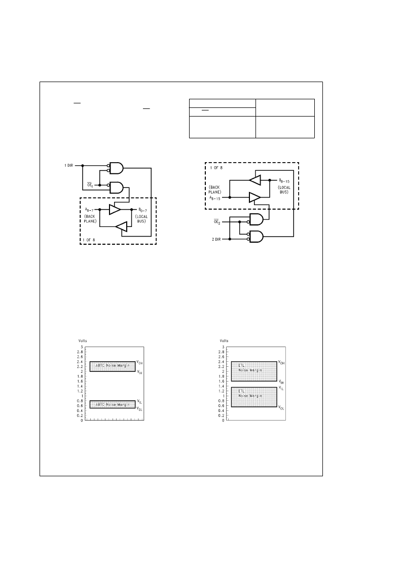
Logic Diagrams
(Positive Logic)
TL/F/11654–3
TL/F/11654–4
ETL’s Improved Noise Immunity
TTL input thresholds are typically determined by tempera-
ture-dependent junction voltages which result in worst case
input thresholds between 0.8V and 2.0V. By contrast, ETL
provides greater noise immunity because its input thresh-
olds are determined by current mode input circuits similar to
those used for ECL or BTL. ETL’s worst case input thresh-
olds, between 1.4V and 1.6V, are compensated for temper-
ature, voltage and process variations.
Incident Wave Switching
When TTL logic is used to drive fully loaded backplanes, the
combination of low backplane bus characteristic imped-
ance, wide TTL input threshold range and limited TTL drive
generally require multiple waveform reflections before a val-
id signal can be received across the backplane. The VME
International Trade Association (VITA) defined ETL to pro-
vide incident wave switching which increases the data trans-
fer rate of a VME backplane and extends the life of VME
applications. TTL compatibility with existing VME back-
planes and modules was maintained.
Improved Input Threshold Characteristics of ETL
TL/F/11654–5
ABTC Worst Case V
OUT
–V
IN
TL/F/11654–6
ETL Worst Case V
OUT
–V
IN
2
相关PDF资料 |
PDF描述 |
|---|---|
| 74F00 | Quad 2-Input NAND Gate(四2输入与非门) |
| 74F02 | Quad 2-Input NOR Gate(四2输入或非门) |
| 74F04 | Hex Inverter(六反相器) |
| 74F08 | Quad 2-Input AND Gate(四2输入与门) |
| 74F109 | Dual JK Positive Edge-Triggered Flip-Flop(双通道正向边沿触发的J-K触发器) |
相关代理商/技术参数 |
参数描述 |
|---|---|
| 74F | 制造商:BOURNS 制造商全称:Bourns Electronic Solutions 功能描述:High Q, high self-resonant frequency Varnish coated |
| 74F00 | 制造商:FAIRCHILD 制造商全称:Fairchild Semiconductor 功能描述:Quad 2-Input NAND Gate |
| 74F00D | 制造商:NXP Semiconductors 功能描述:QUAD 2-INPUT NAND GATE |
| 74F00N | 制造商:NXP Semiconductors 功能描述: |
| 74F00PC | 功能描述:逻辑门 Qd 2-Input NAND Gate RoHS:否 制造商:Texas Instruments 产品:OR 逻辑系列:LVC 栅极数量:2 线路数量(输入/输出):2 / 1 高电平输出电流:- 16 mA 低电平输出电流:16 mA 传播延迟时间:3.8 ns 电源电压-最大:5.5 V 电源电压-最小:1.65 V 最大工作温度:+ 125 C 安装风格:SMD/SMT 封装 / 箱体:DCU-8 封装:Reel |
发布紧急采购,3分钟左右您将得到回复。