- 您现在的位置:买卖IC网 > PDF目录370129 > 74FCT273PMX (National Semiconductor Corporation) Octal D Flip-Flop PDF资料下载
参数资料
| 型号: | 74FCT273PMX |
| 厂商: | National Semiconductor Corporation |
| 英文描述: | Octal D Flip-Flop |
| 中文描述: | 八路D触发器 |
| 文件页数: | 1/8页 |
| 文件大小: | 168K |
| 代理商: | 74FCT273PMX |
TL/F/10146
5
March 1993
54FCT/74FCT273
Octal D Flip-Flop
General Description
The ’FCT273 has eight edge-triggered D-type flip-flops with
individual D inputs and Q outputs. The common buffered
Clock (CP) and Master Reset (MR) input load and reset
(clear) all flip-flops simultaneously.
The register is fully edge-triggered. The state of each D in-
put, one setup time before the LOW-to-HIGH clock tran-
sition, is transferred to the corresponding flip-flop’s Q out-
put.
All outputs will be forced LOW independently of Clock or
Data inputs by a LOW voltage level on the MR input. The
device is useful for applications where the true output only is
required and the Clock and Master Reset are common to all
storage elements.
Features
Y
I
CC
reduced to 40.0
m
A
Y
Ideal buffer for MOS microprocessor or memory
Y
Eight edge-triggered D flip-flops
Y
Buffered common clock
Y
Buffered, asynchronous master reset
Y
TTL input and output level compatible
Y
TTL levels accept CMOS levels
Y
I
OL
e
48 mA (Com), 32 mA (Mil)
Y
NSC 54/74FCT273 is pin and functionally equivalent to
IDT 54/74FCT273
product
compliant
Standard Military Drawing
Y
5962-87656
Y
Military
to
MIL-STD-883
and
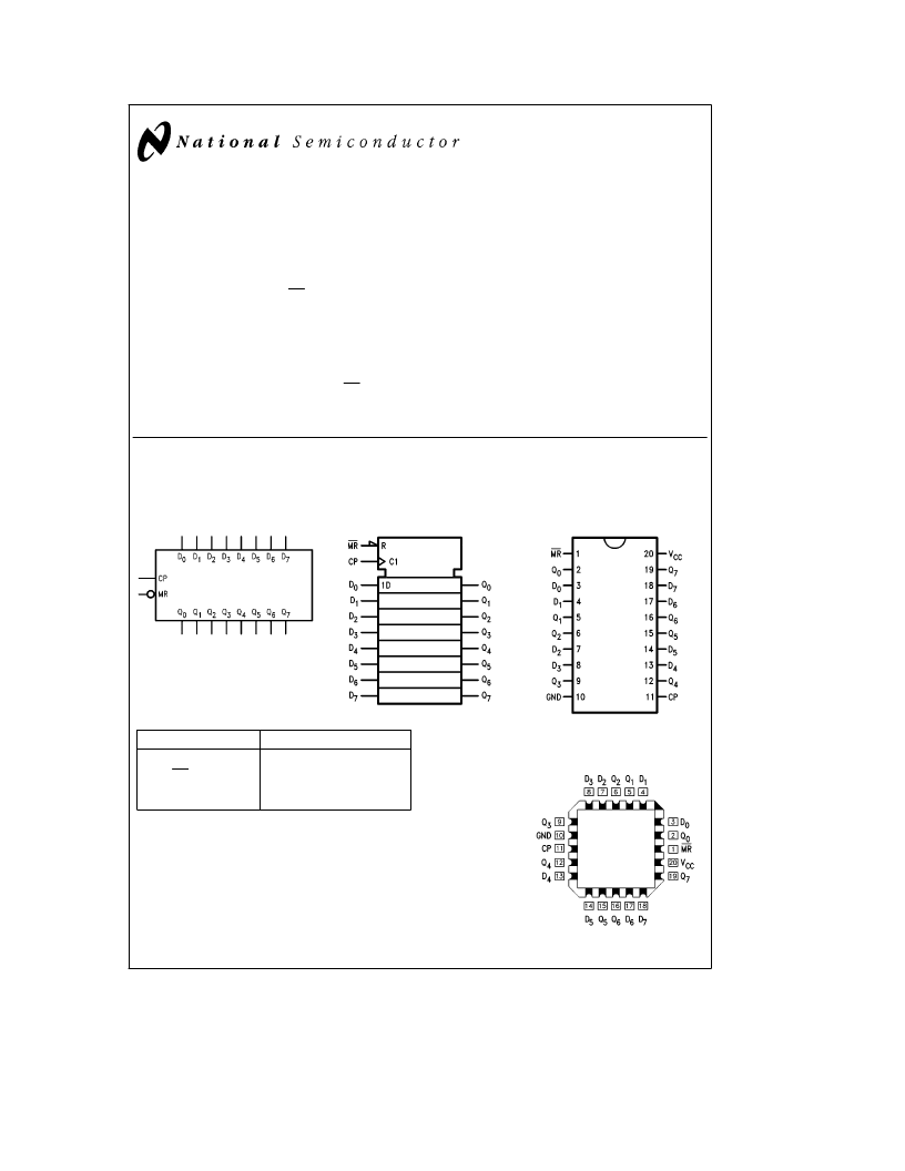
Logic Symbols
Connection Diagrams
TL/F/10146–1
IEEE/IEC
TL/F/10146–2
Pin Assignment
for DIP, Flatpak and SOIC
TL/F/10146–3
Pin Names
Description
D
0
–D
7
MR
CP
Q
0
–Q
7
Data Inputs
Master Reset
Clock Pulse Input
Data Outputs
Pin Assignment
for LCC
TL/F/10146–4
FACT
TM
is a trademark of National Semiconductor Corporation.
C
1995 National Semiconductor Corporation
RRD-B30M105/Printed in U. S. A.
相关PDF资料 |
PDF描述 |
|---|---|
| 74FCT273SCQB | Octal D Flip-Flop |
| 74FCT273SCQR | Octal D Flip-Flop |
| 74FCT273PCQR | Octal D Flip-Flop |
| 74FCT273PMQB | Octal D Flip-Flop |
| 74FCT273PMQR | Octal D Flip-Flop |
相关代理商/技术参数 |
参数描述 |
|---|---|
| 74FCT273SC | 制造商:Rochester Electronics LLC 功能描述:- Bulk |
| 74FCT273SCQB | 制造商:NSC 制造商全称:National Semiconductor 功能描述:Octal D Flip-Flop |
| 74FCT273SCQR | 制造商:NSC 制造商全称:National Semiconductor 功能描述:Octal D Flip-Flop |
| 74FCT273SCX | 制造商:NSC 制造商全称:National Semiconductor 功能描述:Octal D Flip-Flop |
| 74FCT273SMQB | 制造商:NSC 制造商全称:National Semiconductor 功能描述:Octal D Flip-Flop |
发布紧急采购,3分钟左右您将得到回复。