- 您现在的位置:买卖IC网 > PDF目录370130 > 74FST3126QSR (ON SEMICONDUCTOR) 4-Bit Bus Switch PDF资料下载
参数资料
| 型号: | 74FST3126QSR |
| 厂商: | ON SEMICONDUCTOR |
| 元件分类: | 通用总线功能 |
| 英文描述: | 4-Bit Bus Switch |
| 中文描述: | CBT/FST/QS/5C/B SERIES, QUAD 1-BIT DRIVER, TRUE OUTPUT, PDSO16 |
| 封装: | QSOP-16 |
| 文件页数: | 4/8页 |
| 文件大小: | 80K |
| 代理商: | 74FST3126QSR |
74FST3126
http://onsemi.com
4
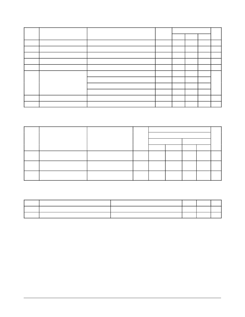
DC ELECTRICAL CHARACTERISTICS
V
CC
T
A
=
40 C to
85 C
Symbol
Parameter
Conditions
(V)
Min
Typ*
Max
Unit
V
IK
Clamp Diode Resistance
I
IN
=
18mA
4.5
1.2
V
V
IH
High–Level Input Voltage
4.0 to 5.5
2.0
V
V
IL
Low–Level Input Voltage
4.0 to 5.5
0.8
V
I
I
Input Leakage Current
0
V
IN
5.5 V
5.5
1.0
A
I
OZ
OFF–STATE Leakage Current
0
A, B
V
CC
5.5
1.0
A
R
ON
Switch On Resistance (Note 6)
V
IN
= 0 V, I
IN
= 64 mA
4.5
4
7
V
IN
= 0 V, I
IN
= 30 mA
4.5
4
7
V
IN
= 2.4 V, I
IN
= 15 mA
4.5
8
15
V
IN
= 2.4 V, I
IN
= 15 mA
4.0
11
20
I
CC
Quiescent Supply Current
V
IN
= V
CC
or GND, I
OUT
= 0
5.5
3
A
I
CC
Increase In I
CC
per Input
*Typical values are at V
CC
= 5.0 V and T
A
= 25 C.
6. Measured by the voltage drop between A and B pins at the indicated current through the switch.
One input at 3.4 V, Other inputs at V
CC
or GND
5.5
2.5
mA
AC ELECTRICAL CHARACTERISTICS
Limits
T
A
=
40 C to
85 C
V
CC
= 4.5 to 5.5 V
V
CC
= 4.0 V
Symbol
Parameter
Conditions
Figures
Min
Max
Min
Max
Unit
t
PHL
,
t
PLH
Prop Delay Bus to Bus
(Note 7)
V
I
= OPEN
4 and 5
0.25
0.25
ns
t
PZH
,
t
PZL
Output Enable Time
V
I
= 7 V for t
PZL
V
I
= OPEN for t
PZH
4 and 5
1.0
4.5
5.0
ns
t
PHZ
,
t
PLZ
Output Disable Time
V
I
= 7 V for t
V
I
= OPEN for t
PHZ
4 and 5
1.5
5.7
6.2
ns
7. This parameter is guaranteed by design but is not tested. The bus switch contributes no propagation delay other than the RC delay of the
typical On resistance of the switch and the 50 pF load capacitance, when driven by an ideal voltage source (zero output impedance).
CAPACITANCE
(Note 8)
Symbol
Parameter
Conditions
Typ
Max
Unit
C
IN
Control Pin Input Capacitance
V
CC
= 5.0 V
3
pF
C
I/O
8. T
A
=
Input/Output Capacitance
V
CC
= 5.0 V, OE = 0 V
5
pF
25 C, f = 1 MHz, Capacitance is characterized but not tested.
相关PDF资料 |
PDF描述 |
|---|---|
| 74FST3126 | ADAPTERS, COAX; FME JACK TO MINI UHF FEMALE COAXIAL ADAPTER |
| 74FST3244 | 8-Bit Bus Switch |
| 74FST3244DT | 8-Bit Bus Switch |
| 74FST3244DTR2 | 8-Bit Bus Switch |
| 74FST3244DW | 8-Bit Bus Switch |
相关代理商/技术参数 |
参数描述 |
|---|---|
| 74FST32384Q | 制造商:Rochester Electronics LLC 功能描述:- Bulk 制造商:Integrated Device Technology Inc 功能描述: |
| 74FST32390Q | 制造商:Rochester Electronics LLC 功能描述:- Bulk |
| 74FST3244 | 制造商:ONSEMI 制造商全称:ON Semiconductor 功能描述:8−Bit Bus Switch |
| 74FST3244/D | 制造商:未知厂家 制造商全称:未知厂家 功能描述:8-Bit Bus Switch |
| 74FST3244_06 | 制造商:ONSEMI 制造商全称:ON Semiconductor 功能描述:8−Bit Bus Switch |
发布紧急采购,3分钟左右您将得到回复。