参数资料
| 型号: | 74HC1G32GW,125 |
| 厂商: | NXP Semiconductors |
| 文件页数: | 11/11页 |
| 文件大小: | 0K |
| 描述: | IC 2-INPUT OR GATE SC88A-5 |
| 产品培训模块: | Logic Packages |
| 标准包装: | 1 |
| 系列: | 74HC |
| 逻辑类型: | 或门 |
| 电路数: | 1 |
| 输入数: | 2 |
| 电源电压: | 2 V ~ 6 V |
| 电流 - 静态(最大值): | 20µA |
| 输出电流高,低: | 2.6mA,2.6mA |
| 逻辑电平 - 低: | 0.5 V ~ 1.8 V |
| 逻辑电平 - 高: | 1.5 V ~ 4.2 V |
| 额定电压和最大 CL 时的最大传播延迟: | 23ns @ 6V,50pF |
| 工作温度: | -40°C ~ 125°C |
| 安装类型: | 表面贴装 |
| 供应商设备封装: | 5-TSSOP |
| 封装/外壳: | 6-TSSOP(5 引线),SC-88A,SOT-353 |
| 包装: | 标准包装 |
| 其它名称: | 568-7732-6 |
CS35L01/03
DS909F1
9
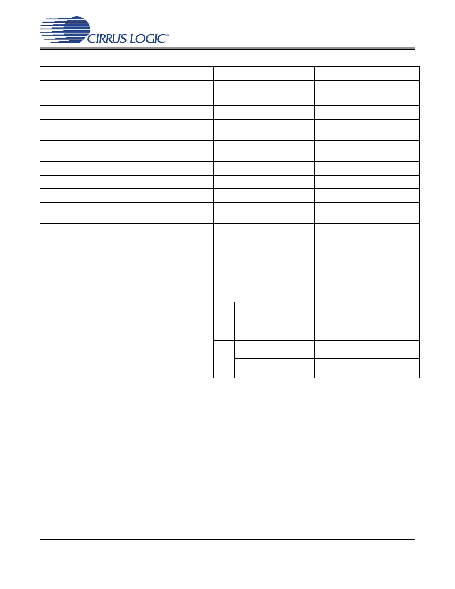
ELECTRICAL CHARACTERISTICS - ALL OPERATIONAL MODES
Note:
6. No external loads should be connected to the LFILT+ net. Any connection of a load to this point may
result in errant operation or performance degradation in the device.
7. When VBATT is below this threshold (VBLIM), operation is automatically restricted to SD mode.
8. When operating in HD or FHD mode and the differential input voltage remains below the input level
threshold (VIN-LDO) for a period of time (tLDO), the PWM outputs will be powered by the internally
generated LDO supply (VLDO).
9. When operating in HD or FHD mode and the differential input voltage is above this input level
threshold (VIN-VBATT), the PWM outputs will be powered directly from the VBATT supply.
10. Refer to Section 5.5 for more information on Thermal Error functionality.
11. Under Voltage Lockout is the threshold at which a decreasing VBATT supply will disable device
operation.
Parameters
Symbol
Test Conditions
Min
Typ
Max Units
Max. Current from LFILT+
ILFILT+
-10
-
A
LFILT+ Output Impedance
ZLFILT+
-0.7
-
VBATT Limit for HD/FHD Mode
VBLIM
-3.0
-
VDC
Input Level for Entering LDO Operation in
HD/FHD Modes
VIN-LDO
CS35L03
CS35L01
-
0.015VBATT
0.029VBATT
-
Vrms
Input Level for Entering VBATT Operation in
HD/FHD Modes
VIN-VBATT
CS35L03
CS35L01
-
0.09
0.19
-
Vrms
LDO Entry Time Delay
tLDO
-
1200
-
ms
LDO Level for HD/FHD Modes
VLDO
-1.0
-
V
Output Offset Voltage
VOFFSET Inputs AC coupled to GND
-+/-1.5
-
mV
Amplifier Gain
AV
CS35L03
CS35L01
-
12
6
-
dB
Shutdown Supply Current
IA(SD)
SD = Low
-0.05
-
A
MOSFET On Resistance
RDS(ON) Ibias = 0.5 A
-270
-
m
Thermal Error Threshold
TTE
-150
-
C
Thermal Error Retry Time
RTE
-100
-
ms
Under Voltage Lockout Threshold
UVLO
-
2.0
-
V
Operating Efficiency
Output Levels at 10% THD+N
8
+
33
H
Load
VBATT = 5 VDC
-
92
-
%
VBATT = 3.7 VDC
-
91
-
%
4
+
33
H
Load
VBATT = 5 VDC
-
87
-
%
VBATT = 3.7 VDC
-
86
-
%
相关PDF资料 |
PDF描述 |
|---|---|
| 74HC1G00GW,125 | IC 2-IN NAND GATE SC88A-5 |
| OSTVK141150 | CONN TERM BLK HDR 14POS 3.5MM |
| OSTOQ203250 | CONN TERM BLK HDR 20POS 3.81MM |
| OSTOQ203251 | CONN TERM BLK HDR 20POS 3.81MM |
| OSTOQ201250 | CONN TERM BLK HEADER 20POS 3.5MM |
相关代理商/技术参数 |
参数描述 |
|---|---|
| 74HC1G32GW-G | 功能描述:逻辑门 2-INPUT OR GATE RoHS:否 制造商:Texas Instruments 产品:OR 逻辑系列:LVC 栅极数量:2 线路数量(输入/输出):2 / 1 高电平输出电流:- 16 mA 低电平输出电流:16 mA 传播延迟时间:3.8 ns 电源电压-最大:5.5 V 电源电压-最小:1.65 V 最大工作温度:+ 125 C 安装风格:SMD/SMT 封装 / 箱体:DCU-8 封装:Reel |
| 74HC1G32GW-Q100H | 制造商:NXP Semiconductors 功能描述:74HC1G32GW-Q100/UMT5/REELR// - Tape and Reel 制造商:NXP Semiconductors 功能描述:IC GATE OR 2-INPUT 5TSSOP 制造商:NXP Semiconductors 功能描述:OR Gate 1-Element 2-IN CMOS 5-Pin TSSOP T/R |
| 74HC1G32GW-R | 功能描述:逻辑门 2-INPUT OR GATE RoHS:否 制造商:Texas Instruments 产品:OR 逻辑系列:LVC 栅极数量:2 线路数量(输入/输出):2 / 1 高电平输出电流:- 16 mA 低电平输出电流:16 mA 传播延迟时间:3.8 ns 电源电压-最大:5.5 V 电源电压-最小:1.65 V 最大工作温度:+ 125 C 安装风格:SMD/SMT 封装 / 箱体:DCU-8 封装:Reel |
| 74HC1G66 | 制造商:PHILIPS 制造商全称:NXP Semiconductors 功能描述:Bilateral switch |
| 74HC1G665GV125 | 制造商:NXP 功能描述: 制造商:NXP Semiconductors 功能描述: |
发布紧急采购,3分钟左右您将得到回复。