参数资料
| 型号: | 74HC374N,652 |
| 厂商: | NXP Semiconductors |
| 文件页数: | 8/8页 |
| 文件大小: | 0K |
| 描述: | IC FLIP FLOP OCT D 3STATE 20DIP |
| 产品培训模块: | Logic Packages |
| 标准包装: | 720 |
| 系列: | 74HC |
| 功能: | 标准 |
| 类型: | D 型总线 |
| 输出类型: | 三态非反相 |
| 元件数: | 1 |
| 每个元件的位元数: | 8 |
| 频率 - 时钟: | 83MHz |
| 延迟时间 - 传输: | 14ns |
| 触发器类型: | 正边沿 |
| 电源电压: | 2 V ~ 6 V |
| 工作温度: | -40°C ~ 125°C |
| 安装类型: | 通孔 |
| 封装/外壳: | 20-DIP(0.300",7.62mm) |
| 包装: | 管件 |
74LVCH32245A
All information provided in this document is subject to legal disclaimers.
NXP B.V. 2011. All rights reserved.
Product data sheet
Rev. 5 — 15 December 2011
8 of 15
NXP Semiconductors
74LVCH32245A
32-bit bus transceiver with direction pin; 5 V tolerant; 3-state
[1]
Typical values are measured at Tamb =25 C and VCC = 1.2, 1.8, 2.5 V, 2.7 V, and 3.3 V respectively.
[2]
tpd is the same as tPLH and tPHL.
ten is the same as tPZL and tPZH.
tdis is the same as tPLZ and tPHZ.
[3]
Skew between any two outputs of the same package switching in the same direction. This parameter is guaranteed by design.
[4]
CPD is used to determine the dynamic power dissipation (PD in W).
PD =CPD VCC2 fi N+ (CL VCC2 fo) where:
fi = input frequency in MHz; fo = output frequency in MHz
CL = output load capacitance in pF
VCC = supply voltage in Volts
N = number of inputs switching
(C
L VCC
2
f
o) = sum of the outputs.
11. Waveforms
tdis
disable time
nOE to nAn, nBn; see Figure 5
VCC = 1.2 V
-
11.0
-
ns
VCC = 1.65 V to 1.95 V
1.5
4.9
13.1
1.5
14.7
ns
VCC = 2.3 V to 2.7 V
0.5
2.7
7.1
0.5
7.9
ns
VCC = 2.7 V
1.5
3.4
6.6
1.5
8.5
ns
VCC = 3.0 V to 3.6 V
1.5
3.3
5.6
1.5
7.0
ns
tsk(o)
output skew
time
VCC = 3.0 V to 3.6 V
-
1.0
-
1.5
ns
CPD
power
dissipation
capacitance
per buffer; VI =GND to VCC
VCC = 1.65 V to 1.95 V
-
11.5
-
pF
VCC = 2.3 V to 2.7 V
-
15.2
-
pF
VCC = 3.0 V to 3.6 V
-
18.5
-
pF
Table 7.
Dynamic characteristics …continued
Voltages are referenced to GND (ground = 0 V). For test circuit see Figure 6.
Symbol Parameter
Conditions
Tamb = 40 C to +85 C 40 C to +125 C Unit
Min
Typ[1]
Max
Min
Max
VM = 1.5 V at VCC 2.7 V.
VM =0.5 VCC at VCC <2.7 V.
VOL and VOH are typical output voltage levels that occur with the output load.
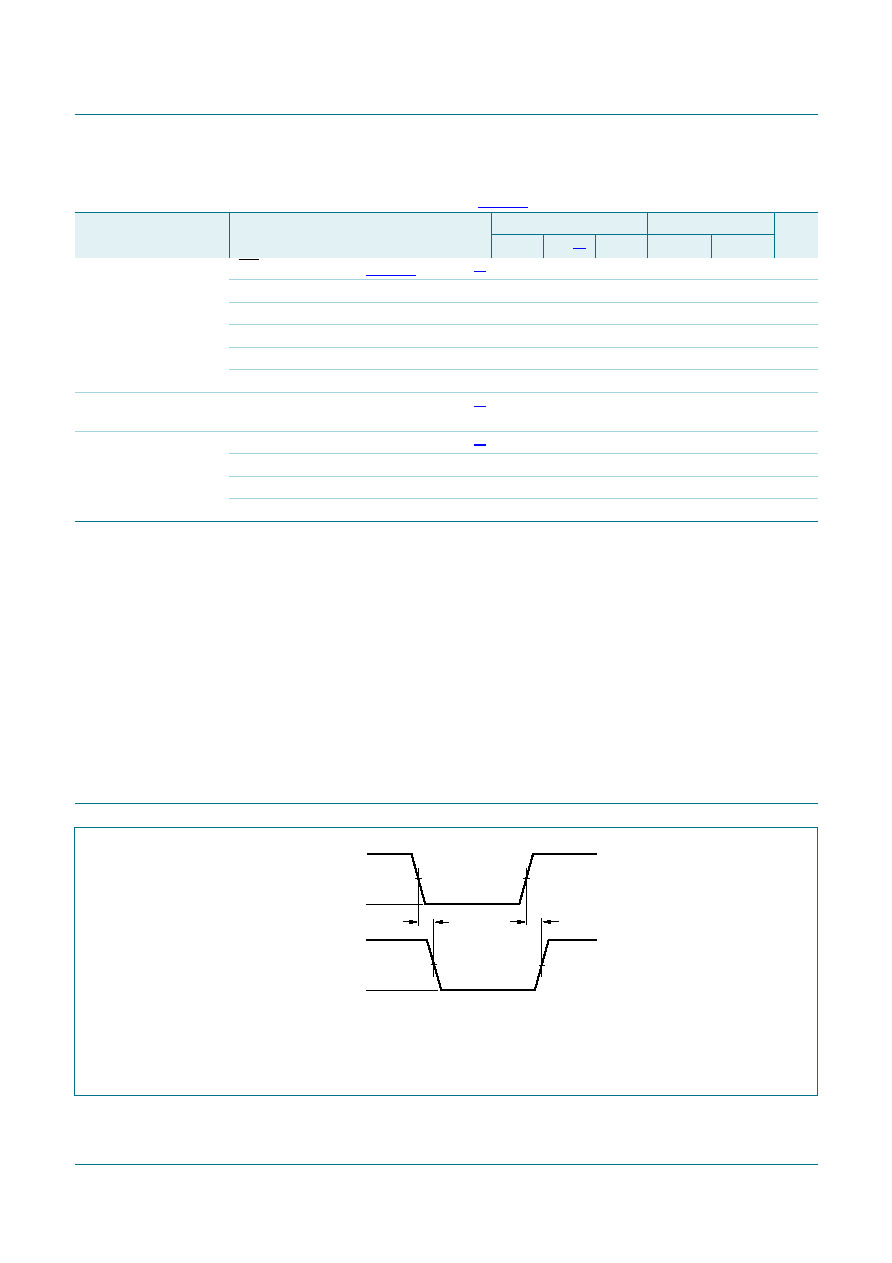
Fig 4.
The input (nAn, nBn) to output (nBn, nAn) propagation delays
mna477
nAn, nBn
input
nBn, nAn
output
tPHL
tPLH
GND
VI
VM
VOH
VOL
相关PDF资料 |
PDF描述 |
|---|---|
| SY10EL07ZC TR | IC GATE XOR/XNOR 2-INPUT 8-SOIC |
| 74HC273N,652 | IC FLIP FLOP OCT D RESET 20DIP |
| 74HCT273N,652 | IC FLIP FLOP OCT D RESET 20DIP |
| SY10EL07ZC | IC GATE XOR/XNOR 2-INPUT 8-SOIC |
| 74HCT174N,652 | IC FLIP FLOP HEX D RESET 16DIP |
相关代理商/技术参数 |
参数描述 |
|---|---|
| 74HC374NSGS 89 | 制造商:SGS 功能描述:74HC374N |
| 74HC374NSGS89 | 制造商:SGS 功能描述:74HC374N |
| 74HC374PV-E | 制造商:Renesas Electronics 功能描述:Cut Tape 制造商:Renesas 功能描述:Flip Flop D-Type Bus Interface Pos-Edge 3-ST 1-Element 20-Pin PDIP Tube |
| 74HC374PW | 功能描述:触发器 OCTAL D 3-S RoHS:否 制造商:Texas Instruments 电路数量:2 逻辑系列:SN74 逻辑类型:D-Type Flip-Flop 极性:Inverting, Non-Inverting 输入类型:CMOS 输出类型: 传播延迟时间:4.4 ns 高电平输出电流:- 16 mA 低电平输出电流:16 mA 电源电压-最大:5.5 V 最大工作温度:+ 85 C 安装风格:SMD/SMT 封装 / 箱体:X2SON-8 封装:Reel |
| 74HC374PW,112 | 功能描述:触发器 OCTAL D 3-S RoHS:否 制造商:Texas Instruments 电路数量:2 逻辑系列:SN74 逻辑类型:D-Type Flip-Flop 极性:Inverting, Non-Inverting 输入类型:CMOS 输出类型: 传播延迟时间:4.4 ns 高电平输出电流:- 16 mA 低电平输出电流:16 mA 电源电压-最大:5.5 V 最大工作温度:+ 85 C 安装风格:SMD/SMT 封装 / 箱体:X2SON-8 封装:Reel |
发布紧急采购,3分钟左右您将得到回复。