- 您现在的位置:买卖IC网 > PDF目录76122 > 74HC4352N (NXP SEMICONDUCTORS) 4-CHANNEL, DIFFERENTIAL MULTIPLEXER, PDIP20 PDF资料下载
参数资料
| 型号: | 74HC4352N |
| 厂商: | NXP SEMICONDUCTORS |
| 元件分类: | 多路复用及模拟开关 |
| 英文描述: | 4-CHANNEL, DIFFERENTIAL MULTIPLEXER, PDIP20 |
| 封装: | PLASTIC, DIP-20 |
| 文件页数: | 9/16页 |
| 文件大小: | 125K |
| 代理商: | 74HC4352N |
December 1990
2
Philips Semiconductors
Product specication
Dual 4-channel analog
multiplexer/demultiplexer with latch
74HC/HCT4352
FEATURES
Wide analog input voltage range: ± 5V.
Low “ON” resistance:
80
(typ.) at VCC VEE = 4.5 V
70
(typ.) at VCC VEE = 6.0 V
60
(typ.) at VCC VEE = 9.0 V
Logic level translation:
to enable 5 V logic to communicate with
± 5 V analog
signals
Typical “break before make” built in
Address latches provided
Output capability: non-standard
ICC category: MSI
GENERAL DESCRIPTION
The 74HC/HCT4352 are high-speed Si-gate CMOS
devices. They are specified in compliance with JEDEC
standard no. 7A.
The 74HC/HCT4352 are dual 4-channel analog
multiplexers/demultiplexers with common select logic.
Each multiplexer has four independent inputs/outputs
(nY0 to nY3) and a common input/output (nZ).
The common channel select logics include two select
inputs (S0 and S1), an active LOW enable input (E1), an
active HIGH enable input (E2) and a latch enable input
(LE).
With E1 LOW and E2 HIGH, one of the four switches is
selected (low impedance ON-state) by S0 and S1. The data
at the select inputs may be latched by using the active
LOW latch enable input (LE). When LE is HIGH, the latch
is transparent. When either of the two enable inputs, E1
(active LOW) and E2 (active HIGH), is inactive, all analog
switches are turned off.
VCC and GND are the supply voltage pins for the digital
control inputs (S0, S1, LE, E1 and E2). The VCC to GND
ranges are 2.0 to 10.0 V for HC and 4.5 to 5.5 V for HCT.
The analog inputs/outputs (nY0 to nY3, and nZ) can swing
between VCC as a positive limit and VEE as a negative limit.
VCC VEE may not exceed 10.0 V.
For operation as a digital multiplexer/demultiplexer, VEE is
connected to GND (typically ground).
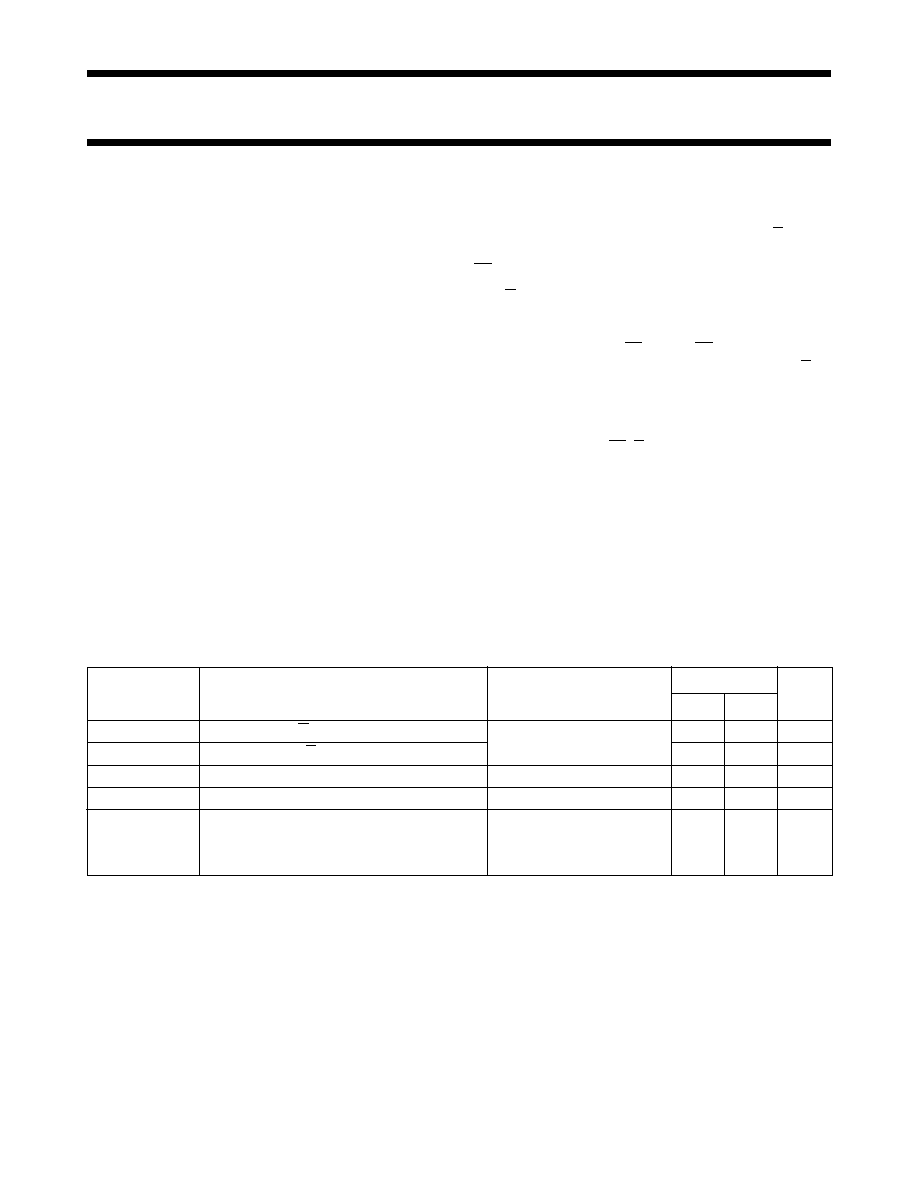
QUICK REFERENCE DATA
VEE = GND = 0 V; Tamb =25 °C; tr =tf = 6 ns
Notes
1. CPD is used to determine the dynamic power dissipation (PD in W):
PD =CPD × VCC2 × fi +∑ { (CL + CS )× VCC2 × fo } where:
fi = input frequency in MHz
fo = output frequency in MHz
∑ {(CL + CS)× VCC2 × fo } = sum of outputs
CL = output load capacitance in pF
CS = max. switch capacitance in pF
VCC = supply voltage in V
2. For HC the condition is VI = GND to VCC
For HCT the condition is VI = GND to VCC 1.5 V
SYMBOL
PARAMETER
CONDITIONS
TYPICAL
UNIT
HC
HCT
tPZH/ tPZL
turn “ON” time E1, E2 or Sn to Vos
CL = 15 pF; RL =1k;
VCC =5 V
31
33
ns
tPHZ/ tPLZ
turn “OFF” time E1, E2 or Sn to Vos
20
ns
CI
input capacitance
3.5
pF
CPD
power dissipation capacitance per switch
notes 1 and 2
55
pF
CS
max. switch capacitance
independent (Y)
5
pF
common (Z)
12
pF
相关PDF资料 |
PDF描述 |
|---|---|
| 74HC4352D-T | 4-CHANNEL, DIFFERENTIAL MULTIPLEXER, PDSO20 |
| 74HC4067U | 16-CHANNEL, SGL ENDED MULTIPLEXER, UUC |
| 74HC4316U | QUAD 1-CHANNEL, SGL POLE SGL THROW SWITCH, UUC |
| 7702807XX | 1-OUTPUT TWO TERM VOLTAGE REFERENCE, 3.3 V, BCY2 |
| 74LV4799SN | 1-CHANNEL POWER SUPPLY SUPPORT CKT, PDIP16 |
相关代理商/技术参数 |
参数描述 |
|---|---|
| 74HC4353D | 功能描述:多路器开关 IC TRIPLE 2-CHANNEL MUS/DEMUS/WL RoHS:否 制造商:Texas Instruments 通道数量:1 开关数量:4 开启电阻(最大值):7 Ohms 开启时间(最大值): 关闭时间(最大值): 传播延迟时间:0.25 ns 工作电源电压:2.3 V to 3.6 V 工作电源电流: 最大工作温度:+ 85 C 安装风格:SMD/SMT 封装 / 箱体:UQFN-16 |
| 74HC4353D,652 | 功能描述:多路器开关 IC TRIPLE 2-CHANNEL RoHS:否 制造商:Texas Instruments 通道数量:1 开关数量:4 开启电阻(最大值):7 Ohms 开启时间(最大值): 关闭时间(最大值): 传播延迟时间:0.25 ns 工作电源电压:2.3 V to 3.6 V 工作电源电流: 最大工作温度:+ 85 C 安装风格:SMD/SMT 封装 / 箱体:UQFN-16 |
| 74HC4353D,653 | 功能描述:多路器开关 IC TRIPLE 2-CHANNEL RoHS:否 制造商:Texas Instruments 通道数量:1 开关数量:4 开启电阻(最大值):7 Ohms 开启时间(最大值): 关闭时间(最大值): 传播延迟时间:0.25 ns 工作电源电压:2.3 V to 3.6 V 工作电源电流: 最大工作温度:+ 85 C 安装风格:SMD/SMT 封装 / 箱体:UQFN-16 |
| 74HC4353D-T | 功能描述:多路器开关 IC TRIPLE 2-CHANNEL MUS/DEMUS/WL RoHS:否 制造商:Texas Instruments 通道数量:1 开关数量:4 开启电阻(最大值):7 Ohms 开启时间(最大值): 关闭时间(最大值): 传播延迟时间:0.25 ns 工作电源电压:2.3 V to 3.6 V 工作电源电流: 最大工作温度:+ 85 C 安装风格:SMD/SMT 封装 / 箱体:UQFN-16 |
| 74HC4353N | 制造商:NXP Semiconductors 功能描述:TRIPLE 1-CHANNEL, SGL ENDED MULTIPLEXER, PDIP20 |
发布紧急采购,3分钟左右您将得到回复。