- 您现在的位置:买卖IC网 > PDF目录8480 > 74HCT109DB,118 (NXP Semiconductors)IC DUAL JK POS-EDG-TRG FF 16SSOP PDF资料下载
参数资料
| 型号: | 74HCT109DB,118 |
| 厂商: | NXP Semiconductors |
| 文件页数: | 2/9页 |
| 文件大小: | 0K |
| 描述: | IC DUAL JK POS-EDG-TRG FF 16SSOP |
| 产品培训模块: | Logic Packages |
| 标准包装: | 2,000 |
| 系列: | 74HCT |
| 功能: | 设置(预设)和复位 |
| 类型: | JK 型 |
| 输出类型: | 差分 |
| 元件数: | 2 |
| 每个元件的位元数: | 1 |
| 频率 - 时钟: | 55MHz |
| 延迟时间 - 传输: | 13ns |
| 触发器类型: | 正边沿 |
| 电源电压: | 4.5 V ~ 5.5 V |
| 工作温度: | -40°C ~ 125°C |
| 安装类型: | 表面贴装 |
| 封装/外壳: | 16-SSOP(0.209",5.30mm 宽) |
| 包装: | 带卷 (TR) |
| 其它名称: | 74HCT109DB-T 74HCT109DB-T-ND 935186320118 |
1997 Nov 25
2
Philips Semiconductors
Product specication
Dual JK ip-op with set and reset;
positive-edge trigger
74HC/HCT109
FEATURES
J, K inputs for easy D-type flip-flop
Toggle flip-flop or “do nothing” mode
Output capability: standard
ICC category: flip-flops
GENERAL DESCRIPTION
The 74HC/HCT109 are high-speed Si-gate CMOS devices
and are pin compatible with low power Schottky TTL
(LSTTL). They are specified in compliance with JEDEC
standard no. 7A.
The 74HC/HCT109 are dual positive-edge triggered, JK
flip-flops with individual J, K inputs, clock (CP) inputs, set
(SD) and reset (RD) inputs; also complementary Q and Q
outputs.
The set and reset are asynchronous active LOW inputs
and operate independently of the clock input.
The J and K inputs control the state changes of the
flip-flops as described in the mode select function table.
The J and K inputs must be stable one set-up time prior to
the LOW-to-HIGH clock transition for predictable
operation.
The JK design allows operation as a D-type flip-flop by
tying the J and K inputs together.
Schmitt-trigger action in the clock input makes the circuit
highly tolerant to slower clock rise and fall times.
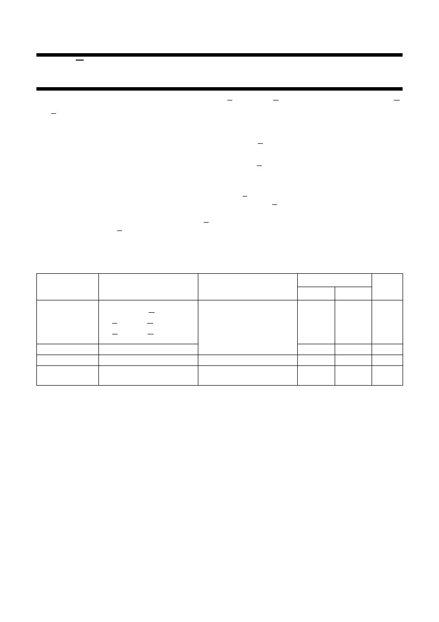
QUICK REFERENCE DATA
GND = 0 V; Tamb = 25 °C; tr = tf = 6 ns
Notes
1. CPD is used to determine the dynamic power dissipation (PD in W):
PD = CPD × VCC2 × fi +∑ (CL × VCC2 × fo) where:
fi = input frequency in MHz
fo = output frequency in MHz
∑ (CL × VCC2 × fo) = sum of outputs
CL = output load capacitance in pF
VCC = supply voltage in V
2. For HC the condition is VI = GND to VCC
For HCT the condition is VI = GND to VCC 1.5 V.
ORDERING INFORMATION
See
“74HC/HCT/HCU/HCMOS Logic Package Information”.
SYMBOL
PARAMETER
CONDITIONS
TYPICAL
UNIT
HC
HCT
tPHL/ tPLH
propagation delay
CL = 15 pF;
VCC = 5 V
nCP to nQ, nQ15
17
ns
nSD to nQ, nQ12
14
ns
nRD to nQ, nQ12
15
ns
fmax
maximum clock frequency
75
61
MHz
CI
input capacitance
3.5
pF
CPD
power dissipation
capacitance per ip-op
notes 1 and 2
20
22
pF
相关PDF资料 |
PDF描述 |
|---|---|
| V300A12M400BG | CONVERTER MOD DC/DC 12V 400W |
| V300A12M400BF3 | CONVERTER MOD DC/DC 12V 400W |
| V300A12M400BF2 | CONVERTER MOD DC/DC 12V 400W |
| MS27502B21CL | RCPT COVER SHELL SIZE 21 CADMIUM |
| M85049/39S25W | STRAIN RELIEF 90 DEG SHELL SZ 25 |
相关代理商/技术参数 |
参数描述 |
|---|---|
| 74HCT109DB-T | 功能描述:触发器 DUAL J-K POS EDGE RoHS:否 制造商:Texas Instruments 电路数量:2 逻辑系列:SN74 逻辑类型:D-Type Flip-Flop 极性:Inverting, Non-Inverting 输入类型:CMOS 输出类型: 传播延迟时间:4.4 ns 高电平输出电流:- 16 mA 低电平输出电流:16 mA 电源电压-最大:5.5 V 最大工作温度:+ 85 C 安装风格:SMD/SMT 封装 / 箱体:X2SON-8 封装:Reel |
| 74HCT109D-Q100J | 功能描述:74HCT109D-Q100/SOT109/SO16 制造商:nexperia usa inc. 系列:* 零件状态:在售 标准包装:2,500 |
| 74HCT109N | 功能描述:触发器 DUAL J-K POS EDGE RoHS:否 制造商:Texas Instruments 电路数量:2 逻辑系列:SN74 逻辑类型:D-Type Flip-Flop 极性:Inverting, Non-Inverting 输入类型:CMOS 输出类型: 传播延迟时间:4.4 ns 高电平输出电流:- 16 mA 低电平输出电流:16 mA 电源电压-最大:5.5 V 最大工作温度:+ 85 C 安装风格:SMD/SMT 封装 / 箱体:X2SON-8 封装:Reel |
| 74HCT109N,652 | 功能描述:触发器 DUAL J-K POS EDGE RoHS:否 制造商:Texas Instruments 电路数量:2 逻辑系列:SN74 逻辑类型:D-Type Flip-Flop 极性:Inverting, Non-Inverting 输入类型:CMOS 输出类型: 传播延迟时间:4.4 ns 高电平输出电流:- 16 mA 低电平输出电流:16 mA 电源电压-最大:5.5 V 最大工作温度:+ 85 C 安装风格:SMD/SMT 封装 / 箱体:X2SON-8 封装:Reel |
| 74HCT109N652 | 制造商:NXP Semiconductors 功能描述:IC JK FLIP FLOP DUAL 14-DIP |
发布紧急采购,3分钟左右您将得到回复。