- 您现在的位置:买卖IC网 > PDF目录76122 > 74HCT4067U (NXP SEMICONDUCTORS) 16-CHANNEL, SGL ENDED MULTIPLEXER, UUC PDF资料下载
参数资料
| 型号: | 74HCT4067U |
| 厂商: | NXP SEMICONDUCTORS |
| 元件分类: | 多路复用及模拟开关 |
| 英文描述: | 16-CHANNEL, SGL ENDED MULTIPLEXER, UUC |
| 文件页数: | 8/15页 |
| 文件大小: | 121K |
| 代理商: | 74HCT4067U |
September 1993
2
Philips Semiconductors
Product specication
16-channel analog
multiplexer/demultiplexer
74HC/HCT4067
FEATURES
Low “ON” resistance:
80
(typ.) at VCC = 4.5 V
70
(typ.) at VCC = 6.0 V
60
(typ.) at VCC = 9.0 V
typical “break before make” built-in
Output capability: non-standard
ICC category: MSI
GENERAL DESCRIPTION
The 74HC/HCT4067 are high-speed Si-gate CMOS
devices and are pin compatible with the “4067” of the
“4000B” series. They are specified in compliance with
JEDEC standard no. 7A.
The 74HC/HCT4067 are 16-channel analog
multiplexers/demultiplexers with four address inputs (S0 to
S3) , an active LOW enable input (E), sixteen independent
inputs/outputs (Y0 to Y15) and a common input/output (Z).
The ”4067” contains sixteen bidirectional analog switches,
each with one side connected to an independent
input/output (Y0 to Y15) and the other side connected to a
common input/output (Z).
With E LOW, one of the sixteen switches is selected (low
impedance ON-state) by S0 to S3. All unselected switches
are in the high impedance OFF-state. With E HIGH, all
switches are in the high impedance OFF-state,
independent of S0 to S3.
The analog inputs/outputs (Y0 to Y15, and Z) can swing
between VCC as a positive limit and GND as a negative
limit. VCC to GND may not exceed 10 V.
QUICK REFERENCE DATA
GND = 0 V; Tamb = 25 °C; tr = tf = 6 ns
Notes
1. CPD is used to determine the dynamic power dissipation (PD in W):
PD = CPD × VCC2 × fi +∑ { (CL + CS) × VCC2 × fo} where:
fi = input frequency in MHz
fo = output frequency in MHz
∑ {(CL + CS) × VCC2 × fo} = sum of outputs
CL = output load capacitance in pF
CS = max. switch capacitance in pF
VCC = supply voltage in V
2. For HC the condition is VI = GND to VCC
For HCT the condition is VI = GND to VCC 1.5 V
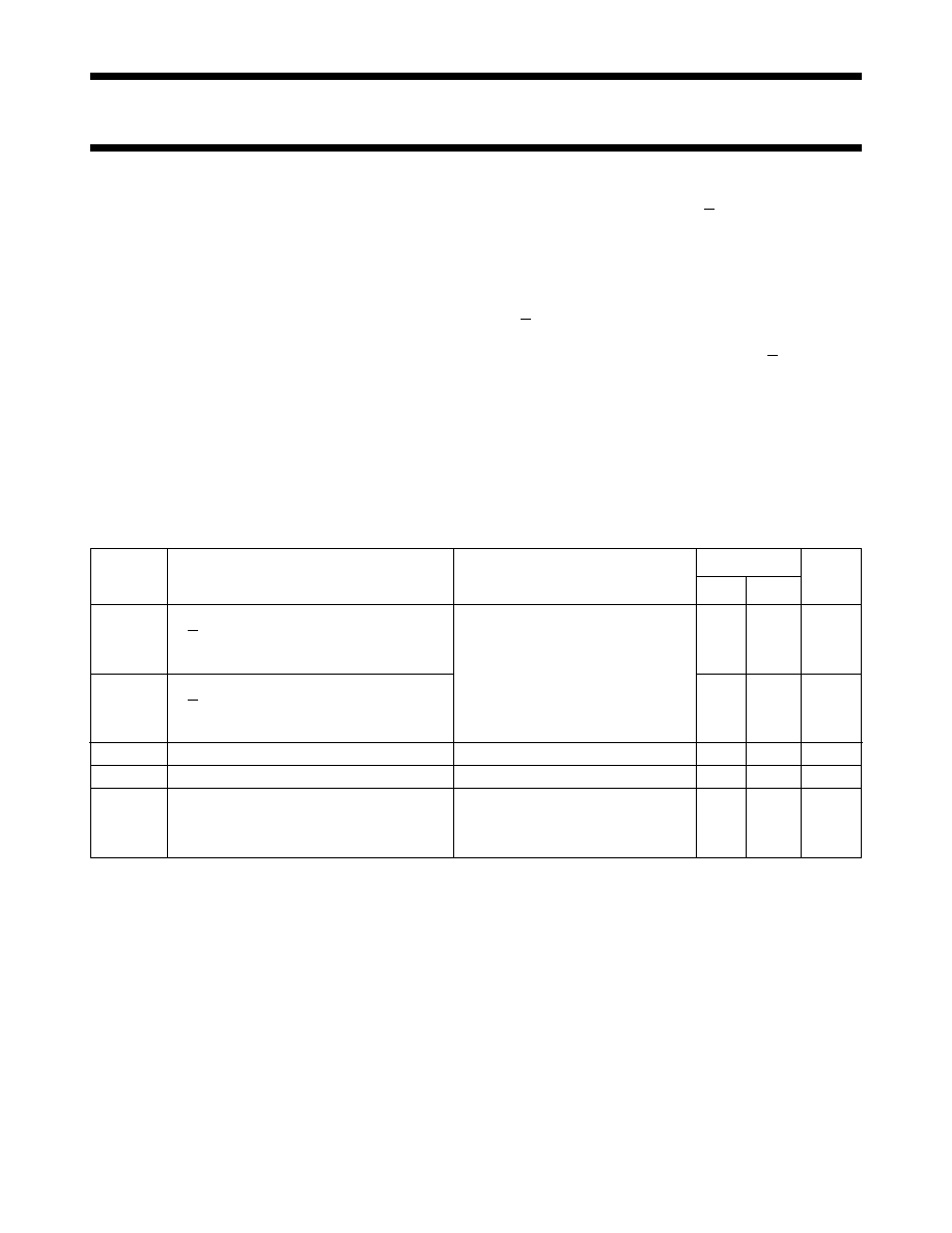
SYMBOL
PARAMETER
CONDITIONS
TYPICAL
UNIT
HC
HCT
tPZL/ tPZH
turn-on time
CL = 15 pF; RL =1 k; VCC = 5 V
E to Vos
26
32
ns
Sn to Vos
29
33
ns
tPLZ/ tPHZ
turn-off time
E to Vos
27
26
ns
Sn to Vos
29
30
ns
CI
input capacitance
3.5
pF
CPD
power dissipation capacitance per switch
notes 1 and 2
29
pF
CS
max. switch capacitance
independent (Y)
5
pF
common (Z)
45
pF
相关PDF资料 |
PDF描述 |
|---|---|
| 74LV4799SD | 1-CHANNEL POWER SUPPLY SUPPORT CKT, PDSO16 |
| 7CR-3012LG | DC-DC REG PWR SUPPLY MODULE |
| 7CR-3012L | DC-DC REG PWR SUPPLY MODULE |
| 7CR-30S120 | DC-DC REG PWR SUPPLY MODULE |
| 74HCT4016U | QUAD 1-CHANNEL, SGL POLE SGL THROW SWITCH, UUC |
相关代理商/技术参数 |
参数描述 |
|---|---|
| 74HCT4075D | 功能描述:逻辑门 TRIPLE 3-IN OR GATE RoHS:否 制造商:Texas Instruments 产品:OR 逻辑系列:LVC 栅极数量:2 线路数量(输入/输出):2 / 1 高电平输出电流:- 16 mA 低电平输出电流:16 mA 传播延迟时间:3.8 ns 电源电压-最大:5.5 V 电源电压-最小:1.65 V 最大工作温度:+ 125 C 安装风格:SMD/SMT 封装 / 箱体:DCU-8 封装:Reel |
| 74HCT4075D,652 | 功能描述:逻辑门 TRIPLE 3-IN OR GATE RoHS:否 制造商:Texas Instruments 产品:OR 逻辑系列:LVC 栅极数量:2 线路数量(输入/输出):2 / 1 高电平输出电流:- 16 mA 低电平输出电流:16 mA 传播延迟时间:3.8 ns 电源电压-最大:5.5 V 电源电压-最小:1.65 V 最大工作温度:+ 125 C 安装风格:SMD/SMT 封装 / 箱体:DCU-8 封装:Reel |
| 74HCT4075D,653 | 功能描述:逻辑门 TRPL 3-INPUT OR GATE RoHS:否 制造商:Texas Instruments 产品:OR 逻辑系列:LVC 栅极数量:2 线路数量(输入/输出):2 / 1 高电平输出电流:- 16 mA 低电平输出电流:16 mA 传播延迟时间:3.8 ns 电源电压-最大:5.5 V 电源电压-最小:1.65 V 最大工作温度:+ 125 C 安装风格:SMD/SMT 封装 / 箱体:DCU-8 封装:Reel |
| 74HCT4075DB | 功能描述:逻辑门 TRIPLE 3-INPUT OR GATE RoHS:否 制造商:Texas Instruments 产品:OR 逻辑系列:LVC 栅极数量:2 线路数量(输入/输出):2 / 1 高电平输出电流:- 16 mA 低电平输出电流:16 mA 传播延迟时间:3.8 ns 电源电压-最大:5.5 V 电源电压-最小:1.65 V 最大工作温度:+ 125 C 安装风格:SMD/SMT 封装 / 箱体:DCU-8 封装:Reel |
| 74HCT4075DB,112 | 功能描述:逻辑门 TRIPLE 3-INPUT OR RoHS:否 制造商:Texas Instruments 产品:OR 逻辑系列:LVC 栅极数量:2 线路数量(输入/输出):2 / 1 高电平输出电流:- 16 mA 低电平输出电流:16 mA 传播延迟时间:3.8 ns 电源电压-最大:5.5 V 电源电压-最小:1.65 V 最大工作温度:+ 125 C 安装风格:SMD/SMT 封装 / 箱体:DCU-8 封装:Reel |
发布紧急采购,3分钟左右您将得到回复。